
| Home | About Us | Contribute | Bookstore | Advertising | Subscribe for Free NOW! |
| News Archive | Features | Events | Recruitment | Directory |
CMP PROCESSING
Learn more about R&D chemical mechanical polishing by requesting our FREE informational CD.

| FREE subscription |
| Subscribe for free to receive each issue of Semiconductor Today magazine and weekly news brief. |
News
9 October 2007
Toshiba presents GaN power FET with record Ku-band output power
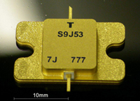
At this week’s European Microwave Conference 2007 in Munich, Germany, Tokyo-based Toshiba Corp is presenting a new gallium nitride power field-effect transistor (FET) with record output power in the Ku-band (12-18GHz) frequency range of 65.4W at 14.5GHz. Key characteristics include linear gain of 8.2dB, a drain voltage of 30V, a chip size of 3.4mm x 0.53mm, and a package size of 21.0mm x 12.9mm.
The main application will be in base-stations for radar and satellite microwave communications, which carry high-capacity signals (including high-definition broadcasts). Ever-increasing communications flows are driving demand for higher output power in signal amplifying devices, as is the development of more powerful radar systems.
Advances in Ku-band microwave amplifiers focus on replacing electron tubes (conventionally used at this bandwidth) with semiconductors. In particular, both for the replacement of electron tubes and for new equipment, Toshiba says that demand is growing steadily for GaN power FETs, which offer advantages over established gallium arsenide devices in heat dissipation and high-power performance characteristics at high microwave frequencies.
 Toshiba directed its initial efforts in GaN power FETs for microwave frequency applications to developing and marketing devices for the 6GHz band (in 2005) and the 9.5GHz band (in 2006), achieving record output power at those frequencies. The firm has now extended its line-up to 14.5GHz.
The record performance of the new power FET was achieved by optimizing the composition and thickness of the AlGaN and GaN layers in its high-electron-mobility transistor (HEMT) structure (formed on a highly heat-conductive silicon carbide substrate). To ensure high performance at Ku-band frequencies, Toshiba applied a shorter gate length of below 0.3 microns, and optimized the shape of each electrode and element configuration to enhance heat dissipation.
However, as gate lengths shorten, suppression of current leakage at the gate electrode is essential for achieving high performance. Toshiba therefore applied a unique overcoat process around each gate electrode, contributing to the suppression of gate leakage to just a thirtieth of the firm´s conventional approaches. To ensure stable processing of gate lengths below 0.3 microns, electron-beam exposure is used.
Also, to reduce parasitic inductance and hence improve high-frequency performance, Toshiba replaced source wire bonding by developing a unique technology for via holes, which form a connection through the chip from the front-side surface source electrode to the back-side ground electrode. Success in forming via holes in SiC substrate, recognized as a highly demanding process, is a breakthrough in development of the new FET, Toshiba claims. The firm also improved the overall design of the matching circuit for practical application at Ku-band frequencies.
Due to the demand for GaN power FETs for radar and satellite microwave communication base-stations , Toshiba is targeting early commercialization of the new Ku-band device. The firm plans to start sample shipment by the end of 2007 and to enter mass production by the end of March 2008.
Meanwhile, Toshiba says it will continue development of GaN power FETs for the 18-30GHz frequencies (Ka-band) and beyond.
See related item:
Toshiba launches X-band GaN HEMT for radar and medical applications
Search: Base stations GaN FET
Visit: www.toshiba.co.jp
![]() ©2007 Juno Publishing and Media Solutions Ltd. All rights reserved. Semiconductor Today and the editorial material contained within it and related media is the copyright of Juno Publishing and Media Solutions Ltd. Reproduction in whole or part without permission from Juno Publishing and Media Solutions Ltd is forbidden. In most cases, permission will be granted, if the author, magazine and publisher are acknowledged.
©2007 Juno Publishing and Media Solutions Ltd. All rights reserved. Semiconductor Today and the editorial material contained within it and related media is the copyright of Juno Publishing and Media Solutions Ltd. Reproduction in whole or part without permission from Juno Publishing and Media Solutions Ltd is forbidden. In most cases, permission will be granted, if the author, magazine and publisher are acknowledged.
Disclaimer: Material published within Semiconductor Today and related media does not necessarily reflect the views of the publisher or staff. Juno Publishing and Media Solutions Ltd and its staff accept no responsibility for opinions expressed, editorial errors and damage/injury to property or persons as a result of material published.
Semiconductor Today, Juno Publishing and Media Solutions Ltd, Suite no. 133, 20 Winchcombe Street, Cheltenham, GL52 2LY, UK
Web site by No Name No Slogan ![]()