| Home | About Us | Contribute | Bookstore | Advertising | Subscribe for Free NOW! |
| News Archive | Features | Events | Recruitment | Directory |
New MEMS White Paper
Download the latest Logitech white paper and learn more about MEMS processing technology and techniques

| FREE subscription |
| Subscribe for free to receive each issue of Semiconductor Today magazine and weekly news brief. |
News
21 June 2007
Photonic crystal yields high-efficiency room-temperature CW GaInAsP nanolaser
Scientists at Yokohama National University in Japan have fabricated what is claimed to be the first continuous-wave (CW) operation at room temperature for the smallest nanometer-scale laser reported to date, using a photonic crystal structure etched into a GaInAsP/InP quantum well to produce stable, highly efficient near-infrared light emission (Nozaki et al, Optics Express, vol. 15, issue 12, pp7506-7514).
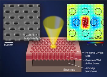
The overall device has a width of several microns, but the active region emitting laser light has dimensions on the nanometer scale in all directions. The laser uses only a microwatt of power (one of the smallest operating powers ever achieved, it is claimed).
The laser's small size and efficiency were made possible by employing the photonic-crystal laser design (first demonstrated at the California Institute of Technology in 1999). After drilling a repeating pattern of holes through the laser material to create a photonic-crystal slab, the researchers introduced an irregularity (defect) into the crystal pattern, e.g. by slightly shifting the positions of adjacent holes. Together, the photonic crystal pattern and the defect exclude light waves of most colors (frequencies) from the structure, except for a small band of frequencies that can exist in the region near the defect. The photonic-crystal slab therefore enables the formation of an ultrasmall laser cavity with a modal volume close to the diffraction limit of light.
For lasers that depend on quantum-mechanical effects, the random noise associated with even a moderately warm environment usually overwhelms the laser light producing process. Continuous operation is therefore difficult to achieve, because it requires careful management of the device's power consumption and heat dissipation. The thermal resistance of previous nanolasers (as high as 10 6K/W) has therefore prevented operation at room temperature and in a mode where laser light is emitted continuously (rather than a series of pulses). In contrast, room-temperature CW operation has to date only been achieved using larger cavities (of 1–10 microns).
But now, due to its photonic-crystal structure, the Yokohama National University nanolaser has a low threshold for lasing of just 1.2 microWatts, which enables operation at room temperature and in CW mode.
According to researcher Toshihiko Baba, the nanolaser can be operated in two modes, depending which value of quality factor (Q) is chosen. Nanolasers operated in a high-Q mode (20,000) could be useful for optical devices in microchips (optical integrated circuits). In a moderate-Q (1500) configuration, the nanolaser needs just an extremely small amount of external power to bring the device to the threshold of producing laser light. In this near-thresholdless mode of operation, the same technology will allow the emission of very low light levels (even single photons).
Abstract:
![]() ©2007 Juno Publishing and Media Solutions Ltd. All rights reserved. Semiconductor Today and the editorial material contained within it and related media is the copyright of Juno Publishing and Media Solutions Ltd. Reproduction in whole or part without permission from Juno Publishing and Media Solutions Ltd is forbidden. In most cases, permission will be granted, if the author, magazine and publisher are acknowledged.
©2007 Juno Publishing and Media Solutions Ltd. All rights reserved. Semiconductor Today and the editorial material contained within it and related media is the copyright of Juno Publishing and Media Solutions Ltd. Reproduction in whole or part without permission from Juno Publishing and Media Solutions Ltd is forbidden. In most cases, permission will be granted, if the author, magazine and publisher are acknowledged.
Disclaimer: Material published within Semiconductor Today and related media does not necessarily reflect the views of the publisher or staff. Juno Publishing and Media Solutions Ltd and its staff accept no responsibility for opinions expressed, editorial errors and damage/injury to property or persons as a result of material published.
Semiconductor Today, Juno Publishing and Media Solutions Ltd, Suite no. 133, 20 Winchcombe Street, Cheltenham, GL52 2LY, UK
Web site by No Name No Slogan ![]()