| Home | About Us | Contribute | Bookstore | Advertising | Subscribe for Free NOW! |
| News Archive | Features | Events | Recruitment | Directory |
| FREE subscription |
| Subscribe for free to receive each issue of Semiconductor Today magazine and weekly news brief. |
News
30 January 2007
IBM and Intel both announce high-k gate dielectric transistors
Both IBM and Intel have separately announced that they have developed transistors that use a high-dielectric-constant (high-k) gate oxide layer.
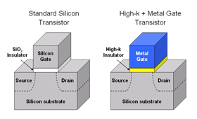
For more than 40 years, ICs have been based on silicon complementary metal-oxide semiconductor (CMOS) transistor technology incorporating a silicon dioxide (SiO2) dielectric layer that insulates the transistor’s conducting channel from the gate electrode (which switches the current flow in the channel on and off). Shrinking the transistors’ dimensions (including the thickness of the gate dielectric layer) has enabled the industry to continue the progression defined by Moore's Law (a doubling every 12-18 months of the number of transistors on a chip, and hence chip performance and function).
However, using the established materials and transistor design, the thickness of the silicon dioxide gate dielectric layer is down to as little as 1.2nm thick (equal to five atomic layers) in Intel’s 65nm process technology. The shrinking leads to increased current leakage through the gate dielectric (causing wastage of electric current and unnecessary heating), recognized as one of the most formidable technical challenges facing Moore’s Law.
For its 45nm transistor technology, Intel replaced the silicon dioxide with a hafnium-based high-k gate dielectric material (deposited using atomic layer deposition). This allows the use of a thicker layer with the same electrical capacitance, reducing current leakage more than 10-fold compared to using silicon dioxide.
However, the high-k gate dielectric is not compatible with existing polysilicon gate electrodes, causing two fundamental problems: threshold voltage pinning (Fermi level pinning) and phonon scattering, which both cause lower transistor performance. Intel has therefore also developed a transistor gate electrode that uses a new combination of unspecified metal materials that are compatible with hafnium (using different combinations for the complementary NMOS and PMOS transistors in CMOS).
Intel claims to be first to implement a combination of high-k gate dielectric and metal gates in 45nm process technology. “The implementation of high-k and metal materials marks the biggest change in transistor technology since the introduction of polysilicon gate MOS transistors in the late 1960s,” says co-founder Gordon Moore.
Intel claims that the combination of the high-k gate dielectric with the metal gate for its 45nm process technology provides more than a 20% increase in drive current (or higher transistor performance) while conversely reducing source-drain current leakage more than five-fold, improving the energy efficiency of the transistor. “Our implementation of novel high-k and metal gate transistors for our 45nm process technology will help Intel deliver even faster, more energy-efficient multi-core products that build upon our successful Intel Core 2 and Xeon family of processors, and extend Moore’s Law well into the next decade,” claims senior fellow Mark Bohr.
Intel already has five early-version 45nm processors working (targeted at five different computer market segments), running Windows1, Vista1, Mac OS X1, Windows1 XP and Linux operating systems, as well as various applications. These are the first of 15 planned 45nm processors (codenamed ‘Penryn’) across desktop, mobile, workstation and enterprise segments. Intel plans to put its new transistors in the next-generation family of Intel Core 2 Duo, Intel Core 2 Quad and Xeon multi-core processors. The firm says it remains on track for 45nm production in second-half 2007.
Picture: Intel's 45nm high-k plus metal gate transistor stack.
Meanwhile, working with AMD and its other development partners Sony and Toshiba, IBM also says it has substituted silicon dioxide with “a new, higher-k gate dielectric material” that provides superior electrical properties, enhancing the transistor's function while allowing its size to be shrunk beyond existing limits. This clears a path toward chip circuitry that is smaller, faster and more power-efficient than previously thought possible, the firm adds.
“Until now, the chip industry was facing a major roadblock in terms of how far we could push current technology,” says Dr T.C. Chen, vice president of Science and Technology, IBM Research. "After more than 10 years of effort, we now have a way forward,” adds Chen. The development should ensure the future of CMOS-based logic using silicon-based transistors and Moore’s Law well into the next decade, the firm reckons.
IBM adds that the technology can be incorporated into existing chip manufacturing lines with minimal changes to tooling and processes, making it economically viable. The firm has already inserted the technology into its manufacturing line in East Fishkill, NY and will apply it to products with chip circuits as small as 45nm starting in 2008.
Visit Intel: http://www.intel.com
Visit IBM: http://www.research.ibm.com
![]() ©2007 Juno Publishing and Media Solutions Ltd. All rights reserved. Semiconductor Today and the editorial material contained within it and related media is the copyright of Juno Publishing and Media Solutions Ltd. Reproduction in whole or part without permission from Juno Publishing and Media Solutions Ltd is forbidden. In most cases, permission will be granted, if the author, magazine and publisher are acknowledged.
©2007 Juno Publishing and Media Solutions Ltd. All rights reserved. Semiconductor Today and the editorial material contained within it and related media is the copyright of Juno Publishing and Media Solutions Ltd. Reproduction in whole or part without permission from Juno Publishing and Media Solutions Ltd is forbidden. In most cases, permission will be granted, if the author, magazine and publisher are acknowledged.
Disclaimer: Material published within Semiconductor Today and related media does not necessarily reflect the views of the publisher or staff. Juno Publishing and Media Solutions Ltd and its staff accept no responsibility for opinions expressed, editorial errors and damage/injury to property or persons as a result of material published.
Semiconductor Today, Juno Publishing and Media Solutions Ltd, Suite no. 133, 20 Winchcombe Street, Cheltenham, GL52 2LY, UK
Web site by No Name No Slogan ![]()