


- News
11 September 2019
Vertical gallium oxide Schottky barrier diodes with improved performance
Researchers based in the USA and Japan claim the highest Baliga figure of merit (FOM) of 0.6GW/cm2 so far for β-phase gallium oxide (Ga2O3) vertical Schottky barrier diodes (SBDs) [Noah Allen et al, IEEE Electron Device Letters, published online 29 July 2019]. The breakdown voltage was 1100V.
The Baliga FOM measures the trade-off between breakdown voltage (BV) and on-resistance. The reported value is competitive with state-of-the-art gallium nitride (GaN) and silicon carbide (SiC) SBDs. One previous report of a Ga2O3 SBD gave a Baliga FOM of 0.39GW/cm2 with a 2.44kV breakdown voltage.
The team from Virginia Polytechnic Institute and State University and the University of Southern California in the USA, Novel Crystal Technology Inc in Japan, and the US Naval Research Laboratory used a small-angle beveled field plate (SABFP) and non-punch-through (NPT) design to achieve the high FOM.
Field plates (FPs) are used to massage electric fields, reducing peak values for a given bias. The NPT design consists of a lightly doped drift layer, which contains all of the space-charge region even at breakdown. In punch-through (PT) designs, by contrast, the space-charge region begins to encroach on the more heavily doped lower region of the device. PT designs enable higher breakdown voltages, but at the cost of higher on-resistance.
The researchers comment: “The NPT design is particularly critical for Ga2O3 devices as it makes them competitive with vertical GaN and SiC devices despite the higher bulk electron mobility in GaN and SiC.”
Ga2O3 is being explored for high-power and high-voltage application due to its high expected critical field of order 8MV/cm, resulting from its ultra-wide bandgap of 4.8eV, compared with 3.3-3.4eV for GaN and SiC. The electron mobility of Ga2O3 is more than 200cm2/V-s. Another attractive feature is the availability of large-diameter Ga2O3 substrates. Novel Crystal Technology has spec sheets for 2-inch diameter and 10mmx15mm substrates.
The Ga2O3 drift layer was grown by halide vapor phase epitaxy (HVPE) on 2-inch tin-doped n+-Ga2O3 substrates (Figure 1). The doping donor concentration (ND) of the drift layer was in the range 3.0-3.5x10¹⁶/cm3.
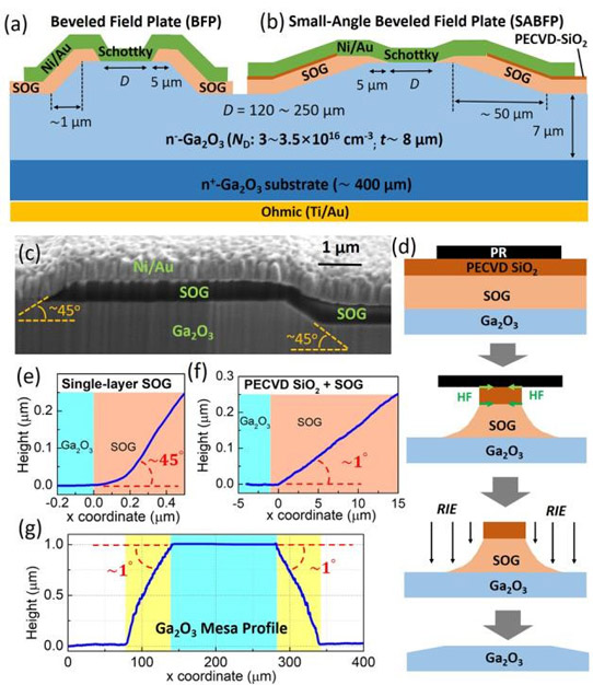
Figure 1: Schematics of vertical Ga2O3 SBDs with (a) BFPs and (b) SABFPs. (c) Cross-sectional scanning electron microscope images of BFP structure. (d) Key process steps for fabricating SABFP structure using SiO2/SOG bilayer mask. SOG surface profiles after wet etch (e) without and (f) with a SiO2 interlayer. (g) Surface profile of Ga2O3 mesa after dry etch using small-angle bilayer mask.
Device fabrication was initiated with thinning the substrate from 652μm to 400μm, using mechanical grinding and polishing/chemical mechanical planarization (CMP). The aim of this step was to reduce series resistance.
Spin-on-glass (SOG) served both as a hard mask for mesa etching and as the field-plate dielectric/support. A 45°-bevel was achieved by hydrofluoric acid wet etching of the SOG hard mask through patterned photoresist (PR), and then inductively coupled plasma etch of the Ga2O3 with boron trichloride reactive ions. The bevel/mesa etch depth was ~1μm.
The shallower bevel structure was obtained using a bilayer mask that consisted of 450nm SOG followed by 200nm of plasma-enhanced chemical vapor deposition (PECVD) silicon dioxide (SiO2). The SiO2 layer speeded up the lateral wet etch under the photoresist through diffusion along the PR/SiO2/SOG interfaces. This enabled reduction of the bevel angle from 45° to 1°.
The devices were completed with the deposition of SOG for the field-plate dielectric, backside annealed titanium/gold Ohmic contact formation, and creation of the Schottky contact/FP with wet etch of an opening in the SOG and nickel/gold deposition.
The 45° (BFP) and 1° SABFP devices were compared against Schottky barrier diodes (SBDs) with no FP and with a standard surface FP (Figure 2).
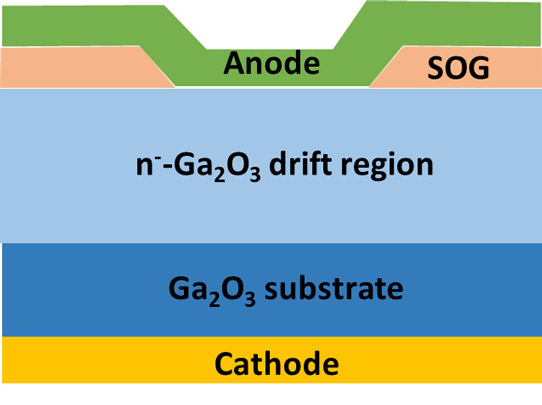
Figure 2: SFP structure.
The SABFP SBD demonstrated an on-off current ratio of almost 109. The ideality was 1.2 – the excess over unity is attributed to lateral inhomogeneity of the Schottky barrier height. The effective barrier height was ~1.2eV. The differential on-resistance (Ron) was ~2mΩ-cm2 normalized according to the Schottky anode area. The comparison devices delivered similar on-resistance performance. The low value was enabled by the reduced substrate thickness.
Destructive breakdown (BV) under reverse bias occurred at 1100V, which compared with 650V, 400V and 200V for the BFP, SFP and no FP SBDs, respectively. Traces of burning were observed at the Schottky contact edges.
Simulations of the SABFP device suggested that the peak electric fields at 1100V reverse bias were 3.5MV/cm in the Ga2O3 and 9MV/cm in the SOG. Experiments on SOG suggested that 9MV/cm was the field point where exponential leakage begins.
The simulations also suggested that, since the depletion region only reached around 7μm into the structure, some reduction in on-resistance could be achieved by reducing the drift layer from 8μm to around 7μm without compromising the NPT design.
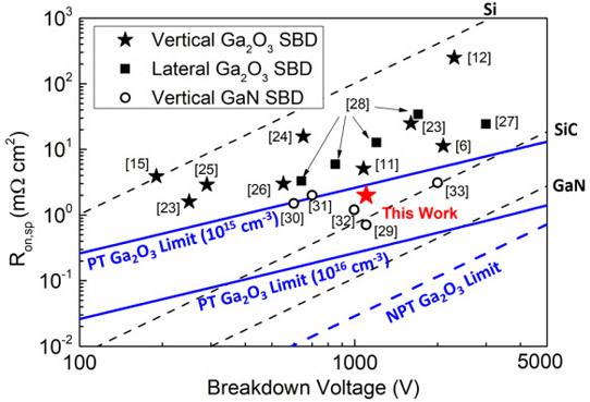
Figure 3: Ron against BV for reported vertical and lateral Ga2O3 SBDs and vertical GaN SBDs. Theoretical limits of Si, SiC, GaN and Ga2O3 NPT, and Ga2O3 PT designs with ND values of 1015/cm3 and 1016/cm3 are plotted. (Ga2O3 limits assume 300cm2/V-s electron mobility and 8MV/cm critical field.)
The team reports (Figure 3): “Our SABFP-SBDs shows a FOM [figure of merit (BV2/Ron)] of 0.6GW/cm2, which is the highest in all Ga2O3 SBDs reported and is comparable to the state-of-the-art vertical GaN SBDs.” The researchers also point out that their simulated peak field of 3.5MV/cm in the Ga2O3 exceeds the critical field in GaN or SiC. Indeed, state-of-the-art vertical GaN SBDs have only achieved less than 3MV/cm.
Vertical gallium oxide Schottky barrier diodes GaO GaN SiC
https://doi.org/10.1109/LED.2019.2931697
The author Mike Cooke is a freelance technology journalist who has worked in the semiconductor and advanced technology sectors since 1997.


