


- News
6 September 2019
Reduced contact resistance aluminium gallium nitride channel power devices
Ohio State University and University of South Carolina in the USA have been developing ohmic contact structures for use with aluminium gallium nitride (AlGaN)-channel electronic devices [Towhidur Razzak et al, Appl. Phys. Lett., vol115, p043502, 2019]. AlGaN is an ultrawide-bandgap semiconductor alloy material that should be able to withstand very large electric fields, enabling high-power and high-voltage applications.
The AlGaN bandgap increases with aluminium content. Pure GaN has been developed for some time for high-power and high-voltage devices, based on its already wide bandgap of ~3.4eV. For Al contents greater than 0.7, the AlGaN bandgap exceeds 5.1eV. Breakdown fields greater than 11MV/cm should thus be possible. However, low resistance to metal contacts is tricky to achieve in high-Al-content AlGaN.
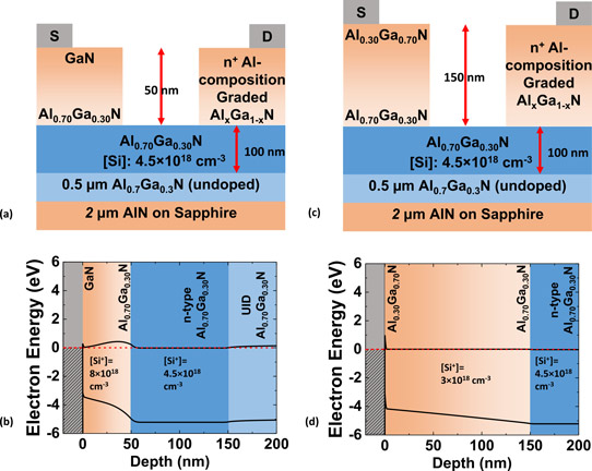
Figure 1: (a) Schematic and (b) energy-band diagram of the access region of sample A with silicon-doping concentration of 8x10¹⁸/cm3, and (c) schematic and (d) energy-band diagram of sample B with 3x10¹⁸/cm3 silicon concentration.
Source-drain contact layers were grown over an Al0.7Ga0.3N channel. Two samples were produced – one (A) where the aluminium content was graded down to zero (GaN=Al0Ga1N) over 50nm, and the other (B) where the grading was to Al0.3Ga0.7N over 150nm (Figure 1). The sample B structure enabled a lower silicon doping to be used to compensate the polarization charge arising from the shallower Al content gradient. The trade-off is between a low metal-semiconductor contact resistance when the Al content at the surface is low (or zero), and high contact layer resistance arising from polarization charge effects.
The samples were grown using metal-organic chemical vapor deposition (MOCVD) on AlN-on-sapphire templates. The source-drain contacts consisted of alloyed titanium/aluminium/nickel/gold. Inductively couple plasma etched out isolation mesas. Selective recessing 60nm into the channel layer defined the active areas of the devices. Hall measurements on sample B gave a channel sheet resistance of 5.6kΩ/square, based on 1.8x10¹³/cm2 sheet carrier density and 56cm2/V-s mobility.
Sample A had non-linear current-voltage characteristics – indicating incomplete compensation of the negative polarization charge in the contact layer by the silicon doping. By contrast, sample B’s characteristic was linear. Sample B’s specific contact resistivity was 3.3x10⁻⁵Ω-cm2, according to transfer-length measurements.
The contact layer resistivity in sample B was estimated at 1x10⁻⁵Ω-cm2, somewhat higher than reported for layers grown by molecular beam epitaxy (MBE). The researchers suggest that this could be due to either non-uniform grading of the contact layer, leading to higher localized polarization charge, and/or non-uniform silicon incorporation.
Sample A was not subjected to Hall or transfer-length analysis due to the non-linear behavior.
The researchers comment (Figure 2) that “the specific contact resistivity obtained for sample B is the lowest observed for any MOCVD-grown AlxGa1-xN-channel devices to date for x > 0.5.”
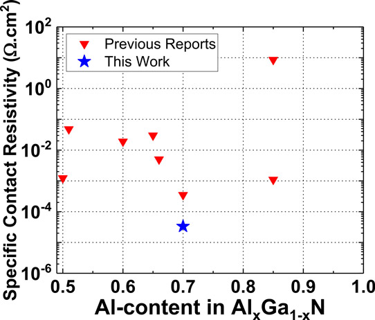
Figure 2: Comparison of specific contact resistivity versus Al-content for state-of-the-art MOCVD-grown AlxGa1-xN-channel transistors with x greater than 0.5.
Sample B was used to create metal-semiconductor field-effect transistor (MESFET) structures with nickel/gold/nickel gates. The gate length was 0.6μm; the source-drain gap was 1.5μm. With 20V drain bias, the peak transconductance was 38mS/mm; pinch-off occurred at -16V gate potential. The maximum drain current was 635mA/mm with +2V gate. This value is claimed as “the highest current density achieved to date for AlxGa1-xN-channel devices with x > 0.5”.
Three-terminal breakdown measurements with the gate at -20V showed no breakdown up to +220V gate-drain potential difference. Combining this with the 0.77μm gate-drain gap gives an average field of 2.86MV/cm - “almost 3x higher than that exhibited by lateral GaN channel devices with similar dimensions,” the researchers say.
The team adds: “The breakdown is mainly limited by the gate leakage current which is the primary contributor to the drain current in the three-terminal breakdown measurement. Thus, the breakdown characteristics can be further improved by the addition of a gate dielectric such as [aluminium oxide,] Al2O3.”
The researchers conclude: “This demonstration provides a technologically important approach to form low-resistance contacts to MOCVD-grown ultrawide-bandgap (UWBG) AlxGa1-xN-channel transistors.”
https://doi.org/10.1063/1.5108529
The author Mike Cooke is a freelance technology journalist who has worked in the semiconductor and advanced technology sectors since 1997.


