


- News
12 September 2019
Monolithic alternating current indium gallium nitride light-emitting chips
Pennsylvania State University in the USA claims the first monolithic integration of high-breakdown Schottky barrier diodes (SBDs) and indium gallium nitride (InGaN) light-emitting diodes (LEDs) to give single chips operated by alternating current (AC) [Jie Liu et al, IEEE Transactions On Electron Devices, published online 8 August 2019]. The 3W device therefore combines the high voltage and light-emitting capabilities of the III-nitride platform. The SBDs are used to convert the AC power source to direct current (DC).
Key to the development was the use of a cyclic etching process involving ‘dry’ plasma and ‘wet’ solution steps to reduce surface defect energy levels interfering with the performance of the SBDs. The researchers comment: “We believe that the approach of fixing the reactive ion etching-induced defects of III-nitrides with cyclic mixed-etching could potentially be extended to the development in micro-LED display devices where the pixelated LEDs suffer from low efficiency due to the presence of high-density surface states on the pixel sidewalls.”
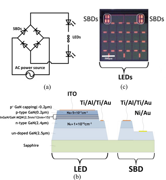
Figure 1: (a) Circuit configuration of AC-LED. (b) Schematic of monolithically integrated LED and SBD. (c) Microphotograph of fabricated AC-LED die.
The epitaxial material used for the AC-LEDs (Figure 1) was from a commercial off-the-shelf product supplied by “a major LED wafer manufacturer”.
Inductively coupled plasma (ICP) etch to a depth of 4.5μm created isolation mesas for the SBD and LED devices. Further ICP etch exposed the n-GaN Ohmic contact regions of the LEDs at a depth of 1.2μm.
The mixed wet/dry etch process was used to remove the LED layers from the SBD mesa, leaving the unintentionally doped GaN surface. Three cycles of the mixed etch was used to give a low density of the surface defects on the unintentionally doped GaN layer of the SBD. The cycle consisted of reactive ion etch using a chlorine-based ICP, followed by boiling potassium hydorxide (KOH) solution. The unetched regions were protected using a patterned nickel hard mask. After the mixed etch, an anneal step raised the temperature to 750°C for 2 minutes in a nitrogen atmosphere.
The p-GaN contact of the LED was indium tin oxide (ITO). The n-GaN contacts of the LED and SBD consisted of titanium/aluminium/titanium/gold (Ti/Al/Ti/Au). These electron-beam evaporated contacts were designed to be Ohmic. The nickel/gold (Ni/Au) Schottky contact on the unintentionally doped GaN was thermally evaporated.
The device surfaces were passivated with plasma-enhanced chemical vapor deposition (PECVD) 500nm-thick silicon dioxide. Contact was made through the passivation using via holes. The metal interconnects for the micro-LED arrays and Schottky diode-based bridge rectifier monolithic circuit consisted of Ti/Al/Ti/Au.
The cyclic etch process gave SBDs with a reverse breakdown voltage of more than 120V, compared with ~27V for devices produced using a conventional etch. The forward voltage of the 120V SBDs was ~2.6V at 20mA injection. The reverse leakage was less than 10μA at 100V bias.
The researchers comment: “The measurement result clearly reveals that the cyclic mixed-etching recipe developed in this work restores the ICP-etched GaN surface to device quality and suppresses the reverse leakage of the Schottky junction of Ni/GaN effectively.” They further suggest that the KOH treatment removes nitrogen vacancies in the GaN, reducing the surface defect donor density.
The micro-LED pixels measured 390μmx325μm. The turn-on voltage for 0.1mA current was 2.56V. The external quantum efficiency was 41.5% at 3.8V and 25mA injection.
Single-chip AC-LED circuits were produced with lateral dimensions of 2.12mmx2mm. The monolithic circuit integrated 28 cascaded micro-LEDs and a bridge rectifier circuit of 8 SBDs. The bridge circuit used 2 SBDs in each branch to handle higher voltages. The SBD had 3 interdigitated Schottky contact fingers that were 20μm wide and spaced at 20μm intervals. The bridge circuit accounted for 11% of the device area. Putting 2 SBDs in each branch enabled rectifying voltages of up 240V, which should be sufficient to enable DC conversion of single-phase US line voltages. The AC-DC conversion efficiency of the bridge circuit was estimated to be 89% from various tests.
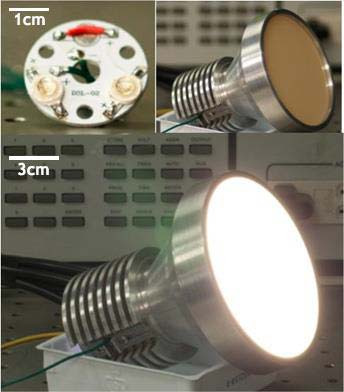
Figure 2: Pictures of packaged AC-LED devices mounted on circuit board and prototype AC-LED lamp with remote phosphor.
The chips were attached to copper heat-sinks with thermally conductive adhesive. Gold wiring connected the devices to the external leads of the packaging. The die was encapsulated in high-refractive-index silicone with a transparent hemispheric plastic cover. The device was then mounted on a printed circuit board and placed in a lamp fixture with a remote phosphor plate with the aim of producing ~5000K white light.
The AC-LED assembly was subjected to 110V root-mean-square (rms) 60Hz power. The measured rms current was 20.6mA with around 82% power factor. The luminous efficacy was 89lm/W. The researchers estimate the heat load of the SBDs at 120VAC was 0.28W, or 9.2% of the overall LED power. The researchers comment: “This power loss is comparable with that (~10%) of a reactive 10%) of a reactive ballast used in compact fluorescent lamps as reported in the general electric technical bulletin. While the incandescent lamps operate in the black-body radiation mode and do not have any drivers as well as the relevant power losses, the luminous efficacy of incandescent lamps is less than 1/5th of the AC-LED lamps reported herein.”
Schottky barrier diodes InGaN LEDs InGaN LEDs GaN
https://doi.org/10.1109/TED.2019.2930467
The author Mike Cooke is a freelance technology journalist who has worked in the semiconductor and advanced technology sectors since 1997.


