


- News
11 September 2019
Wafer-level backside processing of high-frequency indium phosphide chips
Japan’s Nippon Telegraph and Telephone Corp has been working to reduce substrate resonance and ground-bounce effects in indium phosphide (InP)-based chips through wafer-level backside processing [Takuya Tsutsumi et al, IEEE Transactions on Electron Devices, published online 29 July 2019]. The aim is to ensure stable operation of the chips at frequencies needed for sub-millimeter-wavelength electromagnetic radiation and high-speed applications.
The high frequencies of such devices are needed to support future mobile communications: smartphones, 5G, Internet of Things (IoT), autonomous motor vehicles, and so on. The 5G sector is looking to 10Gbits per second data rates using V- and E-band radio frequencies (RFs) of 40–75GHz and 71–76GHz/81–86GHz, respectively. Beyond 5G at 100Gbps data rates, even higher carrier wave frequencies of ~300GHz will be needed.
Also, InP-based integrated circuits (ICs) with high-speed heterojunction bipolar transistors (HBTs) and high-electron-mobility transistors (HEMTs) can be combined with optical emitters and detectors, creating the link between optical fiber and RF networks. The HBT side covers drive circuits for optical transmitters and limiting amplifiers for optical receivers. HEMTs are applied in RF power and low-noise amplifiers.
The ‘ground bounce’ problem refers to instability at high frequency in the ground potential due to feedback through parasitic capacitors and inductors in the body of the device. Ground bounce generates peaks and dips in small-signal response and increases group delay fluctuation. Ground stability can be improved by connecting the IC ground plane to the module ground potential with through-substrate vias or bonding wires.
Substrate resonance is caused by the RF wavelength being of the order of the size of the IC dimensions – millimeter waves can resonate in millimeter chip cavities. The researchers used wafer thinning and dense via structures to reduce these resonance effects.
The process consisted of a number of steps (Figure 1). First the InP wafer was mounted substrate-side up on a glass substrate, using an epoxy-based UV-cured adhesive. The glass mount also included a sacrificial layer to be used later in the demounting step. The InP wafer was thinned through grinding. The final thickness was either 100μm or 50μm – the smaller value was used for higher-frequency performance.
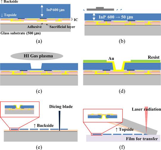
Figure 1: Overview of backside process flow for InP-ICs: (a) mounting on glass substrate; (b) wafer thinning; (c) forming vias by HI-based ICP-RIE; (d) electroplating; (e) backside dicing; and (f) demounting.
Vias were formed using hydrogen iodide (HI) inductively coupled plasma reactive ion etch (HI ICP-RIE). The mask material was polybenzoxazole (PBO). The etch process had an InP etch selectivity ratio of 16, relative to PBO. The temperature was carefully controlled to avoid adhesive degradation. At the same time, the temperature needed to be above 150°C for efficient sublimation of halogenated InP in the material removal process. The team reports that it used an interval cooling step during the etching to precisely and reproducibly control the substrate surface temperature, meeting the rigorous thermal constraints.
The researchers comment: “We obtained an InP etching rate of about 1.5μm/min with good reproducibility with good uniformity across the substrate. With the developed etching sequence, we successfully fabricated the vias without residue, and with good shape uniformity and size controllability.”
Metallization began with the sputtering of a gold (Au) seed layer, followed by selective electroplating of 7μm gold. Unwanted gold seed residue was removed with RIE. The team reports that the electroplated gold was conformal, void-free, and without defects. The gold on the bottom of the vias was 4μm thick, due to micro-loading effects, which also affected the material on the side-walls. The electrical connection between the backside gold and the IC devices was made through the vias.
The researchers achieved 2.5 aspect-ratio (AR) vias in thinner 50μm-thick InP wafers, compared with just 2 AR for 100μm-thick chips. The via diameter could also be reduced to 20μm, compared with 40μm for the 100μm thick chips.
The via diameter was actually tapered, being wider on the backside – in the case of 50μm-diameter vias, the backside diameter was 64μm. The topside diameter (bottom of the via in the etch) was a little less than 50μm in both cases.
According to simulations, vias spaced at 50μm were sufficient to suppress substrate resonance effects.
The chips were diced by sawing through the InP wafer and part of the adhesive layer. The chips were demounted using 1.06μm infrared yttrium aluminium garnet (YAG) laser radiation, which was transmitted through the glass substrate and absorbed by the sacrificial layer.
The team reports: “The adhesive layer and glass substrate can be easily removed because the sacrificial layer is carbonated by the laser irradiation. Since the InP wafer is already diced, ICs are not broken when partial mechanical stress is relieved by removing the adhesive and glass substrate. Thus, we can successfully obtain crack-free InP-IC chips.”
Some negative effects from the laser demounting process were found on InP HBT performance. With the laser power density at 0.31μW/μm2 (just above the minimum needed), the performance was not degraded between that before and after demounting. By contrast, 0.91μW/μm2 irradiation increased base-collector leakage current by more than four orders of magnitude.
InP HEMTs seemed rather more robust to the demounting laser power – with no degradation up to 0.78μW/μm2. At 0.91μW/μm2, there was a slight increase in the maximum drain current with 1.0V bias.
The researchers applied the process to an InP-based HBT limiting amplifier. Such devices could be used in optical receivers for 50Gbps-class NRZ (non-return-to zero) IMDD (intensity modulation direct detection) communication systems.
A 100μm-thick substrate was used since ground-bounce effects were expected to be more important that resonance. Without the backside process, there were dips in the gain-frequency profile of the order 2dB; with the process, the dips were removed giving a smooth curve. The backside process also gave a more consistent group delay with 4ps variation, compared with 14ps for chips without backside processing.
The team comments: “The flatness of the group delay characteristics contributes to improving the waveform quality of RF signals. These experimental results clearly show that thinning the wafer and forming ground vias are effective for achieving stable operation of InP-HBT-based limiting amplifiers with good ground stability.”
The 50μm process was applied to 250GHz InP-HEMT-based sub-millimeter-wave monolithic ICs (SMMICs). The higher frequency was expected to make resonance effects more problematic. These effects were dealt with by incorporating a dense array of vias. The researchers report: “This SMMIC is used as a power amplifier in the transmitter of a wireless communications system. Unlike the case for suppressing ground bounce, the vias are densely formed over the whole surface to cut off the substrate resonance.”
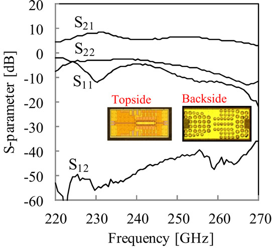
Figure 2: S-parameters of fabricated InP-HEMT-based power amplifier. Inset: topside and backside optical microscope images of InP-HEMT-based power amplifier.
The suppression of resonance enabled a device that showed no dips in its S21 power gain parameter as a function of frequency (Figure 2). Signal isolation (S12) was below -40dB at 250GHz, “thanks to cutting off signals propagating between the input and output ports by vias,” according to the team. Stable amplification was seen between 220GHz and 260GHz with no sign of substrate resonance.
The researchers suggest, based on simulations, that the 50μm process with dense vias could enable frequencies up to 700GHz, beyond the Y-band (325-500GHz) range.
https://doi.org/10.1109/TED.2019.2928849
The author Mike Cooke is a freelance technology journalist who has worked in the semiconductor and advanced technology sectors since 1997.


