


- News
20 September 2019
Gadolinium oxide gate insulation for gallium nitride channel transistors
Researchers from India, Finland and Germany are proposing epitaxial gadolinium oxide (Gd2O3) as a gate insulator for gallium nitride (GaN)-channel metal-oxide-semiconductor high-electron-mobility transistors (MOSHEMTs) [Ritam Sarkar et al, Appl. Phys. Lett.,vol115, p063502, 2019].
The team from the Indian Institute of Technology Bombay, Finland’s Aalto University and Leibniz University in Hannover suggest that the crystalline Gd2O3 should be better able to withstand high-temperature post-deposition treatments than the more usual amorphous oxide gate insulators. At high temperature, amorphous atomic structures tend to become polycrystalline, creating current-leakage paths at grain boundaries, negatively impacting transistor performance. Single-crystal material is more resilient against structural changes at high temperature.
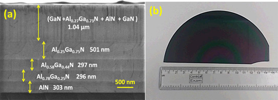
Figure 1: (a) Cross-sectional scanning electron microscope image of AlGaN/GaN heterostructure. (b) Picture of wafer after epitaxial HEMT growth.
With a view to low-cost high-volume manufacturing, the substrate was 1mm-thick 150mm-diameter (111) silicon. Low-pressure metal organic vapor phase epitaxy (MOVPE) produced a step-graded series of AlGaN layers to enable a 1μm (0001) GaN buffer and channel layer (Figure 1). The top aluminium gallium nitride (AlGaN) barrier layers consisted of 1.5nm AlN, 26nm Al0.27Ga0.73N, and 2nm GaN cap.
The Gd2O3 gate oxide was grown by 650°C molecular beam epitaxy (MBE). The sources were Gd2O3 granules evaporated using an electron beam, along with extra molecular oxygen to make up for oxygen depletion from the evaporation process. The III-nitride surface was prepared for the Gd2O3 by heating to 630°C for 30 minutes.
The crystalline nature of the Gd2O3 varied according to the layer thickness: at ~2.8nm the structure was hexagonal, according to high-resolution x-ray diffraction, by 15nm the structure transforms to monoclinic. A mixed state of hexagonal and monoclinic structures was found for 5.5nm thickness.
The x-ray analysis also suggested that the Gd2O3 put the underlying AlGaN under compressive strain along the c-axis of the crystal structure. Hall measurements of sheet carrier density and mobility of the two-dimensional electron gas (2DEG) channel near the AlGaN/GaN interface gave values in the ranges 5-6x10¹²/cm2 and 1400-1500cm2/V-s, respectively. “The small variation in the mobility and electron concentration could be attributed to a minute fluctuation of Al concentration across the large-diameter wafer,” the researchers comment.
The III-nitride epitaxial material was used to fabricate circular HEMTs with annealed titanium/aluminium/nickel/gold ohmic source/drain contacts. A Schottky gate contact was constructed from nickel/gold.
The maximum drain current was 175mA/mm with 4.5V drain bias and the gate potential at 1V. “The relatively low drain saturation current compared to earlier reported results may be attributed to the large perimeter of the devices (source drain distance ~20μm),” the team explains. The threshold of the HEMT device was -2.7V; the peak transconductance was 60mS/mm. The on/off current ratio was 5x10³.
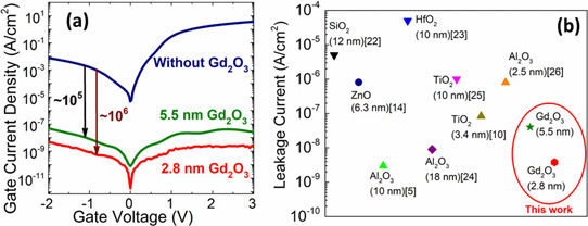
Figure 2: (a) Gate leakage current versus gate voltage for control HEMT and MOSHEMTs with 2.8nm and 5.5nm Gd2O3 thickness. (b) Comparison of leakage current density with earlier reported data on various dielectric-based MOSHEMTs.
Epitaxial material with Gd2O3 allowed fabrication of MOSHEMTs. The gate electrode was tungsten. The insulating Gd2O3 naturally reduced the gate leakage current compared with the Schottky gate on AlGaN of the pure HEMTs by around five orders of magnitude (Figure 2). With 5.5nm Gd2O3, the leakage was ~5x10⁻⁸A/cm2 with the gate at -2V.
Reducing the Gd2O3 to 2.8nm perhaps surprisingly reduced the leakage to ~4x10⁻⁹A/cm2, six orders of magnitude lower than the Schottky HEMT control. The researchers suggest that, unlike thicker layers of Gd2O3, the 2.8nm device benefits from “a single phase (hexagonal) with no domain boundaries, and hence behaves as an ideal oxide with no leakage path”. The 2.8nm Gd2O3 also had the lowest interface trap density (Dit) of ~2.98x10¹²/cm2-eV, according to capacitance-voltage analysis. The dielectric constant of 2.8nm Gd2O3 was ~15.
The Hall sheet carrier density with 2.8nm G2O3 was also enhanced by ~40%. The researchers attribute the boost to in-plane tensile strain from the pseudomorphic Gd2O3 that balances the c-direction compression.
Gadolinium oxide gate insulation GaN MOSHEMT AlGaN MOVPE MBE
https://doi.org/10.1063/1.5109861
The author Mike Cooke is a freelance technology journalist who has worked in the semiconductor and advanced technology sectors since 1997.


