


- News
2 October 2019
Reducing power losses in indium gallium nitride laser diodes on silicon
Researchers in China have reduced the point defects in indium gallium nitride (InGaN) laser diode (LD) material on silicon with the aim of reducing operating voltages and injection current and increasing device efficiency [Jianxun Liu et al, Optics Express, vol. 27, p25943, 2019]. Although silicon-substrate laser diodes benefit from lower cost and raise the prospect of more complex integrated photonics and optoelectronics, efficiencies suffer from the energy-sapping effects of high defect levels.
One problem has been that the lattice mismatch between silicon and gallium nitride (GaN) is about 17%. The thermal expansion mismatch is even greater – around 54%. The lattice/thermal mismatches are now bridged by using various aluminium gallium nitride (AlGaN) alloy layers before the main device layers. Even so, the resulting laser diodes tend to have high threshold currents and voltages, indicating high electrical and optical power losses.
The research team from Suzhou Institute of Nano-Tech and Nano-Bionics (SINANO), University of Science and Technology Beijing, and University of Science and Technology of China, developed a lower-temperature growth process and alternative material structure, in particular layers to reduce threshold currents and voltages by an approximate factor of 2 (72mA/150mA, 4.7V/8.2V).
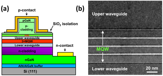
Figure 1: (a) Schematic diagram of InGaN-based laser diodes grown on Si. (b) Cross-sectional high-angle annular dark-field scanning transmission electron micrograph of InGaN MQW active region.
The laser diode material (Figure 1) was grown on (111) silicon with metal-organic chemical vapor deposition (MOCVD). The n-GaN contact layer was 2.7μm, while the lower cladding was 1.2μm n-Al0.05Ga0.95N. The multiple quantum well (MQW) active layer consisted of three pairs of 2.7nm/12nm 770°C In0.12Ga0.88N/In0.02Ga0.98N. The top p-GaN contact was 30nm thick, and the electron layer (EBL) was Al0.2Ga0.8N.
Two laser diode material samples, A and B, were produced (Table 1). Sample B used lower temperatures in the lower and upper waveguides (WGs), and in the p-type contact layer (CL) superlattices (SLs). Lower temperatures reduced thermal degradation of the MQW region and carbon incorporation from the organic precursors used.
Table 1: Comparison of growth conditions between samples A and B.
| Layer/Sample | A | B |
| p-type CL SL, 600nm | 950°C p-Al0.11Ga0.89N/GaN | 920°C p-Al0.11Ga0.89N/GaN |
| Upper WG, 60nm | 1050°C u-GaN | 770°C u-In0.01Ga0.99N/GaN SL |
| Lower WG, 80nm | 1050°C n-GaN | 770°C u-In0.01Ga0.99N/GaN SL |
Carbon tends to compensate, reducing the effectiveness of the magnesium doping used for the p-type layers needed for hole injection. This is expected to increase series resistance and operation voltage, adding to laser diode power losses. Lower carbon levels are also associated with lower optical absorption.
The researchers comment: “It is noted that the adoption of InGaN/GaN SL WG would cause little effect on the thermal conductivity of the laser diode structure, because there was only a trace amount (1% in average) of indium in such SL WGs (sample B), and the total thickness of the In0.01Ga0.99N layer was only 70nm (40 and 30nm for the lower and upper waveguide, respectively), which was negligibly smaller than that of the AlGaN cladding layers (1.8μm in total) and the n-GaN contact layers (2.7μm).”
Due to the lower growth temperatures, microscopic inspection of photoluminescence (PL) in sample B showed greater uniformity, compared with sample A. The more even PL suggests less degradation of the delicate MQW region. In addition, sample A suffered from a short decay time of 3.5ns, compared with 6.3ns for B, in time-resolved PL. The researchers suggest that the faster decay is due to non-radiative Shockley-Read-Hall (SRH) recombination through mid-gap defect levels. The team adds that SRH recombination results in reduced internal quantum efficiency (IQE, photons/electron) and increased junction temperatures and threshold currents.
The researchers also attribute some of the improvement in sample B’s IQE to replacement of the waveguide layer with InGaN SLs. The high-temperature GaN material tends to contain vacancies on the gallium ion site. Reducing the number of vacancies reduces optical absorption from strong band-tail effects. The silicon doping of the n-GaN layer also contributes band-tail energy states. “Such absorption will increase the internal optical loss and reduce the IQE, resulting in an increase in junction temperature and threshold current for the laser diodes,” the team writes.
The team fabricated edge-emitting laser diodes with ridges 800μm long and 4μm wide. The cleaved front and rear facets of the laser diodes were coated with titanium dioxide/silicon dioxide (TiO2/SiO2) multilayers to increase reflectivity with low optical loss.
Electroluminescence experiments (Figure 2) demonstrated lasing peaks at 413.4nm and 418nm for samples A and B, respectively. The laser diodes were operated in 400ns pulse mode with 10kHz repetition to avoid self-heating effects. The wavelength difference is attributed tentatively to differences in MQW growth temperatures, which can significantly affect indium incorporation.
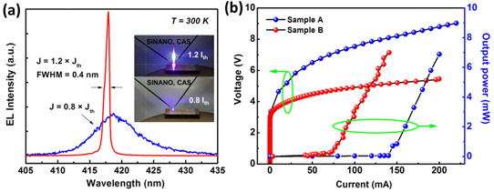
Figure 2: (a) EL spectra of sample B above (1.2x) and below (0.8x) threshold current. Inset: corresponding far-field patterns. (b) On-bar light output power-current-voltage (L-I-V) characteristics under pulsed injection for samples A and B.
Sample B showed a reduced threshold voltage of 4.7V, compared with 8.2V for sample A. The threshold current for B was also about half that of A: 72mA (2.25kA/cm2) versus 150mA (4.7kA/cm2). Reduced current and voltage, and hence input power, for a given output mean increased efficiency.
In lifetime tests under pulsed-mode operation, sample B laser diodes showed little degradation in output power after 620 hours, unlike devices based on sample A material.
InGaN laser diode InGaN AlGaN MOCVD
https://doi.org/10.1364/OE.27.025955
The author Mike Cooke is a freelance technology journalist who has worked in the semiconductor and advanced technology sectors since 1997.


