


- News
2 October 2019
Mitsubishi Electric develops trench-type SiC MOSFET with electric-field-limiting structure
At the International Conference on Silicon Carbide and Related Materials (ICSCRM 2019) in Kyoto, Japan (29 September - 4 October), Tokyo-based Mitsubishi Electric Corp announced that it has developed a trench-type silicon carbide (SiC) metal-oxide-semiconductor field-effect transistor (MOSFET) with a unique electric-field-limiting structure for a power semiconductor device that achieves what is claimed to be record specific on-resistance (at a breakdown voltage of over 1500V) of 1.84mΩ.cm2.
Unique electric-field-limiting structure ensures device reliability
Since SiC MOSFETs control current flowing through the semiconductor layer between the drain and source electrodes by applying a voltage to the gate electrode, in order to achieve control with a small voltage a thin gate-insulating film is required. If a high voltage is applied in a trench-type power semiconductor device, a strong electric field can concentrate in the gate and can easily break the insulating film.
To correct this, Mitsubishi Electric developed a unique electric-field-limiting structure that protects the gate-insulating film by implanting aluminium and nitrogen to change the electrical properties of the semiconductor layer, taking advantage of the trench structure (Figure 1).
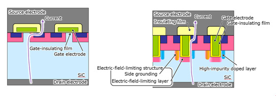
Figure 1: Cross-sectional view of conventional planar SiC-MOSFET (left) and new trench SiC MOSFET (right).
First, aluminium is implanted vertically and an electric-field-limiting layer is formed on the bottom surface of the trench (Figure 2). The electric field applied to the gate-insulating film is reduced to the level of a conventional planar power semiconductor device, improving reliability while maintaining the breakdown voltage of over 1500V.
Next, the side grounding connecting the electric-field-limiting layer and the source electrode is formed (Figure 2) by using a newly developed technique to implant aluminium in an oblique direction to enable high-speed switching and reduced switching loss.
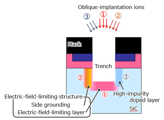
Figure 2: Manufacturing process for trench-type SiC MOSFET.
Locally formed high-impurity doped layers achieve record low on-resistance
The trench SiC MOSFET has transistor cells that are smaller than those of planar types, allowing more cells to be arrayed on a single chip. However, if transistor intervals between the gate electrodes are too narrow then current flow becomes difficult and device resistivity increases. Since Mitsubishi Electric developed a new method for implanting nitrogen in an oblique direction to locally form a layer of SiC with a high concentration of nitrogen, this allows electricity to be conducted easily in the current path (Figure 2). As a result, even when cells are arrayed densely, resistivity can be reduced by about 25% compared with the case of no high-concentration layer.
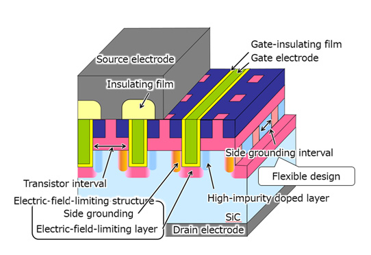
Figure 3: Three-dimensional schematic of new trench-type SiC MOSFET.
The new manufacturing method also allows intervals of the side grounding to be optimized (Figure 3). The result is a specific on-resistance of 1.84mΩ cm2 at room temperature, about half that of planar types, while maintaining a breakdown voltage of over 1500V.
Energy savings and equipment downsizing
Mitsubishi Electric reckons that mounting the transistor in power semiconductor modules for power electronic equipment should lead to energy savings and equipment downsizing.
After improving the performance and confirming the long-term reliability of its new power semiconductor devices, Mitsubishi Electric expects to put its new trench-type SiC MOSFET into practical use sometime after the beginning of fiscal year 2021.
Mitsubishi Electric SiC power MOSFET


