


- News
15 November 2019
Indium gallium nitride surface-emitting superluminescent light diodes
Ireland’s Tyndall National Institute claims a record high 2.2W for output power from indium gallium nitride (InGaN) superluminescent light-emitting diodes (SLEDs) [R. Cahill et al, Appl. Phys. Lett., vol115, p171102, 2019]. The researchers used slanted facets to direct the amplified spontaneous emission (ASE) through the GaN substrate with very low feedback, avoiding laser action. The team also claims that their device is the first surface-emitting structure, since previous reports used edge-emitting geometries.
The team comments: “The surface emitting structure provides potential for integration of further functionality onto the back side of the device, increasing its potential for fiber-based systems and displays.” Other potential uses include high-resolution optical coherence tomography, compact image projectors and smart solid-state lighting.
SLEDs combine the operating principles of LEDs and laser diodes. Lasers generally use Fabry-Perot reflecting structures to feedback light and boost stimulated emission. SLEDs use stimulated emission in a one-pass structure to amplify spontaneously generated photons. The light from SLEDs benefits from features such as high power output and high directionality. A number of strategies are used to suppress feedback, such as absorbing facets or bent cavities.
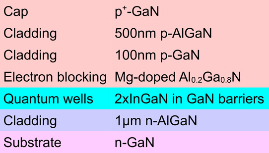
Figure 1: Epitaxial structure.
The Tyndall InGaN material heterostructure was grown on n-GaN substrates using metal-organic vapor phase epitaxy (Figure 1). The fabricated device (Figure 2) consisted of a 3μm-wide waveguide with 1mm gain length. The etched end facets of the waveguide were angled at 45° to form turning mirrors, directing the emitted radiation through the substrate. The back-side of the GaN substrate was polished to minimize scattering of the radiation. A further measure to reduce feedback and increase light extraction was to apply a silicon dioxide anti-reflective layer to the substrate surface.
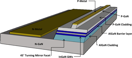
Figure 2: Schematic of blue surface-emitting LED.
The device was operated with 220ns pulses and 1% duty cycle (Figure 3). The maximum output power of 2.2W was achieved at 1.5A injection (50kA/cm2 density). The forward voltage was between 6V and 7V. The external quantum efficiency at the maximum power was 49%. The peak wavelength occurred at 416nm. The researchers comment: “The devices were not observed to degrade under these conditions, testament to the quality of the low-defect-density substrate.”
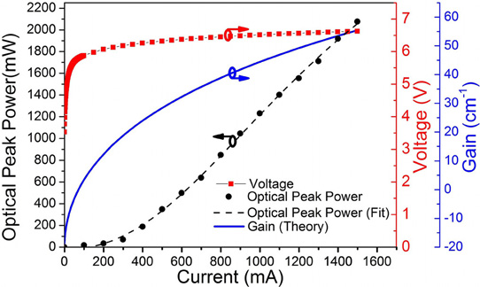
Figure 3: Light–current-voltage and gain characteristics of blue SLED under pulsed operation.
Theoretical analysis using a standard gain model suggested that higher powers could be achieved in future. “The peak optical powers provided by this device are far higher than has been previously reported,” the team writes. The group attributes the high power to the technique for avoiding feedback: directing the radiation through the substrate, rather than using absorbing back facets, for example.
The onset of amplified spontaneous emission occurs for an injection current of about 300mA. At lower current the full-width at half maximum (FWHM) was around 26nm in wavelength. This decreased to the order of 6nm (corresponding to a 41meV energy spread) above 300mA. FWHM values for InGaN lasers tend to be less than 1nm.
The anti-reflective coating was found to suppress parasitic lasing. In devices without such coating, evidence of laser action occurred above 700mA injection.
Analysis of spontaneous emission from the top side of the device suggested active-region heating of the order of 110K between 300mA and 1.5A injection. Also, the study suggested that the carrier temperature increased by about 100K between threshold and maximum power.
Increasing the pulse duration up to 1500ns reduced the output power (~20%) and increased the peak wavelength slightly, indicating the effects of junction heating on the device. The researchers hope that improved thermal management measurements could lead to longer pulse lengths or even continuous-wave operation at higher currents.
InGaN SLEDs MOCVD GaN substrates
https://doi.org/10.1063/1.5118953
The author Mike Cooke is a freelance technology journalist who has worked in the semiconductor and advanced technology sectors since 1997.


