


- News
15 November 2019
Germany-funded ‘ForMikro-GoNext’ project investigating vertical gallium oxide devices for power electronics
In the recently launched joint project ‘ForMikro-GoNext’ - funded by Germany’s Federal Ministry of Education and Research (BMBF) with about €2m over 4 years - the Leibniz-Institut für Kristallzüchtung (IKZ), the Ferdinand-Braun-Institut Leibniz-Institut für Höchstfrequenztechnik (FBH), the University of Bremen and industrial partners ABB Power Grids Switzerland Ltd and Aixtron SE are investigating beta-gallium oxide (β-Ga2O3) using a new vertical device architectures to exploit its properties for transistors more effectively.
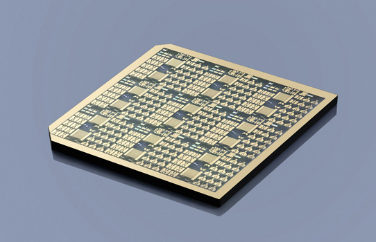
Picture: Gallium oxide chip with lateral transistor and measurement structures, fabricated at FBH by projection lithography. ForMikro-GoNext targets a vertical device architecture. (©FBH/schurian.com)
Wide-bandgap semiconductor materials such as silicon carbide (SiC) and gallium nitride (GaN) offer a higher electrical breakdown field strength than silicon, allowing the fabrication of components in much smaller and more compact dimensions. The semiconductor β-Ga2O3 has a breakdown field strength twice that of SiC and GaN and thus offers the potential to further increase power converter efficiency. High voltages can be switched with significantly smaller semiconductor drift regions - the basis for more compact systems. In addition, transistors based on β-Ga2O3 are characterized by a low on-resistance at a given breakdown voltage and faster switching transients, which leads to lower power losses. Due to these properties, β-Ga2O3 has the best prerequisites to become the high-performance material for next-generation power applications, it is thought.
So far, lateral Ga2O3 devices have been investigated. In this configuration, the voltage is switched across the device surface, making large chip size areas combined with complex isolation techniques necessary for high voltages. ForMikro-GoNext targets vertical device structures in order to more efficiently utilize the high electrical breakdown field strength of β-Ga2O3. Better exploitation of the chip size also opens the potential of upscaling device geometries towards technically relevant very high current level switching. The development of these transistors requires a synchronized process chain from crystal growth, epitaxy and device processing to characterization, which is completely covered within the project.
By focusing the expertise of the Leibniz Institutes IKZ (gallium oxide crystal growth, epitaxy and material characterization) and FBH (device design, manufacturing and testing) the aim is to efficiently transfer the results achieved from basic research into application- and industry-oriented research.
The Institute for Electrical Drives, Power Electronics and Devices (IALB) at the University of Bremen provides qualified assessment of the application potential of the new devices with its power electronic characterization capabilities. Reliability tests will provide information about the stability of the Ga2O3 transistors.
The project will be supported by industrial partners Aixtron (epitaxy) and ABB Power Grids Switzerland Ltd (design and testing of devices).
FBH reports 1.8kV-breakdown gallium oxide MOSFET with record power figure of merit
Ga2O3 Gallium oxide transistors


