


- News
16 May 2019
Ultraviolet aluminium gallium nitride shell nanowire light-emitting diodes
The National Institute of Standards and Technology (NIST) and University of Colorado in the USA have reported aluminium gallium nitride/gallium nitride (AlGaN/GaN) shell/core nanowire light-emitting diodes (LEDs) that demonstrated ~5x the light output compared with GaN/GaN nanowire devices [Matt D Brubaker et al, Nanotechnology, vol30, p234001, 2019].
Developing ultraviolet LEDs such as the 365nm wavelength from the AlGaN/GaN device are seen as being useful for spectroscopy, photopolymer curing, water purification and medical disinfection. Some of these applications need short ‘deep’ UV wavelengths less than 300nm. Nanowire structures might be useful in boosting the pitiful efficiencies (mostly less than 10%) in high-aluminium-content AlGaN LEDs based on conventional technology.
First, ordered arrays of nanowires were grown using plasma-assisted molecular beam epitaxy (PAMBE) on nitrogen-polar GaN/AlN templates on (111) silicon with a silicon nitride mask. The holes in the mask for nanowire growth were 80-240nm diameter with 300-10,000nm pitch. The silicon-doped n-GaN cores were grown at 860°C substrate temperature. The core length was around 2μm. The ~40nm-thick silicon-doped Al0.09Ga0.91N shell was grown at 700°C.
Photoluminescence spectra measured at 5K suggested that the Al mole fraction of the shell tip decreased with nanowire diameter. By contrast, reducing the pitch increased Al concentration. The decrease in Al content at the nanowire tip was related to reduced mobility of the atoms at the growing tip, compared with Ga.
The Al content of the main shell of the nanowire stems was more difficult to determine, probably due to non-radiative recombination, surface states and defects. The researchers used emissions from excitons (bound electron-hole states) to estimate Al content. Smaller-diameter nanowires were found to have higher-Al-content shells. Smaller pitch arrays had low Al concentration.
The nanowire growth process was modified to include doping for p-i-n LEDs. The n-GaN core region was grown to a height of 3.3μm pitched at 5μm. Shell growth was initiated with 15nm n-GaN followed by ~85nm intrinsic AlGaN, ~285nm p-AlGaN and ~5nm heavily doped p++-AlGaN.
The LED p-contact electrode was constructed by 20nm/200nm nickel/gold deposition at normal incidence, followed by 200nm gold at 45°. This covered one side of the wires with metal while the other side allowed light extraction. The n-side current flow was through the buffer with electrical isolation provided by the silicon nitride nanowire growth mask.
The researchers compared the performance of the AlGaN/GaN heterojunction LEDs with GaN/GaN homojunction nanowire devices previously reported by the group (Figure 1). The turn-on voltage of the AlGaN/GaN LEDs was higher than for GaN/GaN, “likely related to the reduced electron overflow current and increased barrier to hole injection expected for higher Al mole fractions,” according to the team.
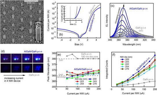
Figure 1: Core–shell p–i–n nanowire LED characteristics comparing AlGaN/GaN heterojunctions and GaN/GaN homojunctions. (a) Scanning electron micrograph of post-metallization AlGaN/GaN core–shell LEDs, with inset pre-metallization single nanowire. (b) Current-voltage characteristics and (c) EL spectra for 25 nanowire LEDs. (d) EL images for 4 nanowire LEDs are shown in the figure. GaN p–i–n EL intensities multiplied by factor of three. (e) Peak emission wavelength and (f) integrated intensity versus current for various core diameters.
Subjecting the AlGaN/GaN LED to prolonged current injection seemed to have an electrical annealing effect on the p-contact, giving increased electroluminescence (EL) intensity and lower series resistance. The researchers comment: “Further development of optimized p-contact metallization and annealing processes are expected to reduce burn-in effects and improve overall device performance.”
The EL from the AlGaN/GaN was around 365nm wavelength, close to the band edge of GaN. This was in contrast to the GaN/GaN LEDs, which emitted around 380nm, corresponding to donor-acceptor-pair (DAP) recombination from electrons injected into the p-GaN shell, according to the researchers. The team also suggests that GaN core emissions could be reabsorbed in the GaN shell, unlike with the wider-bandgap AlGaN.
The 380nm emission and 365nm reabsorption effects are stopped by the wider-bandgap AlGaN, which is also commonly used as an electron-blocking layer in standard GaN LEDs. The researchers report that the integrated EL intensity in the AlGaN/GaN nanowire LEDs was around 5x that of the GaN/GaN reference for a given current injection.
https://doi.org/10.1088/1361-6528/ab07ed
The author Mike Cooke is a freelance technology journalist who has worked in the semiconductor and advanced technology sectors since 1997.


