


- News
23 May 2019
Indium gallium nitride platelets for green and red light-emitting diodes
Lund University and RISE Research Institutes in Sweden have developed indium gallium nitride (InGaN) platelet arrays as a basis for green and red light-emitting diodes (LEDs) [Zhaoxia Bi et al, Nano Lett., published online 2 April, 2019]. The researchers used the platelets to achieve quantum well (QW) regions with higher indium content with less compressive strain from lattice mismatching. “The large strain has a direct impact on the crystal quality of the QWs, potentially introducing plastic crystal deformation during growth and then leading to a dislocation formation,” the team explains.
High strain in InGaN heterostructures also leads to large piezoelectric fields, which reduce the efficiency of the electron-hole recombination processes that are needed for photon emission – a mechanism called the ‘quantum-confined Stark effect’ (QCSE).
Strain effects severely reduce the performance of red and green InGaN-based LEDs, relative to blue devices that can reach 80% external quantum efficiency. By using the InGaN platelets, lower strain in InGaN QWs with high indium content should be achieved due to the smaller lattice mismatch. Higher indium content narrows the bandgap, increasing the wavelength.
The platelet growth technique combined selective-area metal-organic vapor phase epitaxy (MOVPE) and reformation to convert InGaN pyramid structures into c-plane oriented platelets. The selective-area epitaxy was on (0001) GaN-on-silicon templates, using silicon nitride masking with 100nm-diameter holes at 1μm pitch. The platelets are 100-200nm high and extend laterally a few hundred nanometers.
The reformation process consisted of 1070°C annealing in ammonia (NH3) and InGaN regrowth to create a smooth top surface. The annealing did not affect the {10-11} pyramid side facets, which remained smooth after the thermal processing.
The researchers explain: “The surfaces of {10-11} planes are N-terminated. N atoms at the surface are supposed to bond with H atoms cracked from NH3, which can be a reason for the stable {10-11} planes during the annealing.”
The regrowth included an intermediate InGaN layer with a low V/III ratio of 700 (close to the limit for In/Ga droplet formation). The aim of the intermediate layer was to reduce pit formation in the c-plane surface. The researchers suggest that the metal-rich conditions on the growth plane gives a longer adatom diffusion length, flattening the initially rough surface.
The indium content of the intermediate layer was estimated to be less than 5%. The technique was successful in removing pits from In0.09Ga0.91N platelets, but there remained some pits in In0.18Ga0.82N structures. This residual pitting was attributed to the larger lattice mismatch with the intermediate layer. The top InGaN layer was 40-50nm thick.
Comparison of photoluminescence and energy-dispersive x-ray analysis suggested that the InGaN below the intermediate layer had higher indium content fluctuations compared with the InGaN above. Photoluminescence analysis tends to overestimate indium content when there are large fluctuations.
The researchers found that growth of InGaN quantum wells on the InGaN platelets had enhanced indium incorporation, probably due to reduced compressive strain relative to wells grown on pure GaN.
The InGaN platelets had narrow photoluminescence peaks: 107meV and 151meV full-widths at half-maximum (FWHMs) for In0.09Ga0.91N and In0.18Ga0.82N, respectively. These platelets were used for green and red LEDs, respectively.
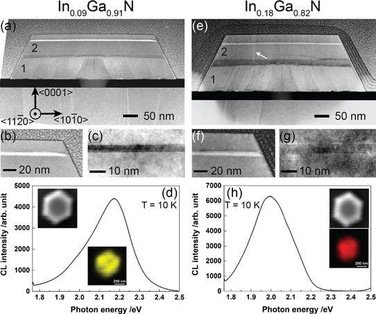
Figure 1: (a, e) Cross-sectional high-angle annular dark-field scanning transmission electron microscope (HAADF-STEM) images of single QW samples. The white arrow in panel e indicates dislocation. (b, f) Magnified HAADF-STEM images close to periphery and (c, g) high-resolution TEM images in middle of QWs. (d, h) CL spectra measured at 10K. Inset: SEM images and corresponding monochromatic CL images with QW emission. CL images recorded in energy windows of (d) 1.80−2.50eV and (h) 1.85−2.35eV.
Cathodoluminescence (CL) spectra under electron-beam excitation showed a QW peak in the emission at 2.17eV (in the yellow range) for the In0.09Ga0.91N platelet and 1.95eV (red) for In0.18Ga0.82N (Figure 1). The researchers report that the QW was slightly thicker on an In0.18Ga0.82N platelet – 5.8nm, compared with 4.5nm. The team suggests the thicker well increases the quantum-confined Stark effect, red-shifting the emission.
The indium content of the well could also be higher on the higher-indium-concentration platelet, narrowing the bandgap. The higher indium content could be the result of reduced ‘indium pulling’ compared with the lower-indium-concentration platelet.
For LEDs, a ~200nm p-InGaN contact layer was added to platelets with quantum wells (Figure 2). The n-contact was through the n-GaN buffer. Electrical isolation was achieved with 30nm atomic layer deposition (ALD) aluminium oxide (Al2O3) passivation and spin-coated/planarized polymer spacer material. The spacer was also used as an etch mask for removal of the Al2O3 from the top of the p-GaN contact. The contact metal was circular in form with 360μm diameter, covering around 1.2x10⁵ platelets.
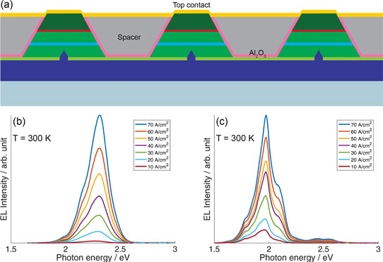
Figure 2: (a) Schematic of InGaN platelet LEDs. (b, c) EL spectra obtained at different current injection levels for green and red LEDs on In0.09Ga0.91N and In0.18Ga0.82N platelets, respectively. Current density normalized to QW rather than contact area.
Electroluminescence (EL) from the LEDs gave green (2.30eV) and red (1.98eV) peaks for In0.09Ga0.91N and In0.18Ga0.82N platelet structures, respectively. The corresponding FWHM linewidths were 210meV and 150meV.
Funding for the work came from various projects: the European Union’s ‘NWs4LIGHT’, the Swedish Foundation for Strategic Research’s ‘Energy-efficient LED-lighting Based on Nanowires’, the Swedish Energy Agency’s ‘Nanowire-based Light Emitting Diodes with Multiple Wavelengths in the Visible Range’, and the EELYS’ ‘Ultra-efficient RGB-lighting Based on Nanowire Technology’. Some money for the work also came from the Swedish Research Council, the Knut and Alice Wallenberg Foundation, and VINNOVA, the Swedish governement’s ‘innovation agency’.
InGaN Red LEDs Green LEDs MOVPE
http://doi.org/10.1021/acs.nanolett.8b04781
The author Mike Cooke is a freelance technology journalist who has worked in the semiconductor and advanced technology sectors since 1997.


