


- News
6 March 2019
Yellow light-emitting diodes with high wall-plug efficiency
Nanchang University and Nanchang Yellow Green Lighting Company Limited in China claim a ‘breakthrough’ in filling the ‘yellow gap’ through the development of high-indium-content indium gallium nitride (InGaN) light-emitting diodes (LEDs) [Fengyi Jiang et al, Photonics Research, vol7, p144, 2019]. The researchers achieved wall-plug efficiencies (WPEs) of 24.3% at 20A/cm2 current injection for 565nm light. At a lower injection of 3A/cm2, the WPE peaked at 33.7%.
The researchers comment: “The success of yellow LEDs can be credited to the improved material quality and reduced compressive strain of InGaN quantum wells by a pre-strained layer and substrate, as well as enhanced hole injection by a 3D pn junction with V-pits.”
Yellow light falls roughly in the wavelength range 560-590nm. While the long (red) and short (violet, blue, cyan, green) sectors of the visible spectrum are relatively well served by light-emitting semiconductors, the central portion (yellow, orange) is difficult to reach with efficient devices.
The long-wavelength LEDs use alloys of aluminium indium gallium arsenide phosphide (AlInGaAsP), while the shorter wavelengths are covered by III-nitrides. However, the efficiency of both these systems drops dramatically as they encroach on the compositions needed for the central part of the visible spectrum.
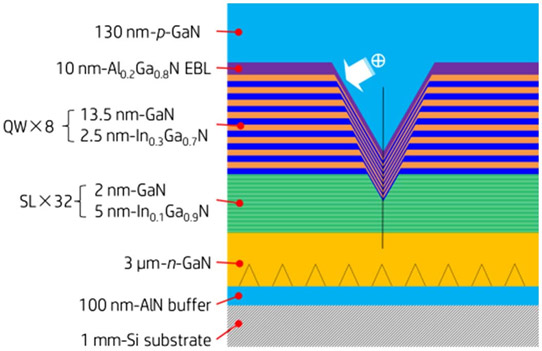
Figure 1: Schematic epitaxial structure of InGaN yellow LED grown on Si substrate.
The researchers used a home-made metal-organic chemical vapor deposition (MOCVD) reactor to apply III-N epitaxial layers to a silicon (111) substrate (Figure 1). The (111) crystal orientation presents a hexagonal template that most closely matches that of III-nitride materials. Even so, there is a large ~17% mismatch in lattice parameters that can lead to threading dislocations and cracked material due to stress. Silicon is attractive as a substrate due to its much lower costs compared with sapphire, silicon carbide, or bulk/freestanding GaN.
The bottom n-GaN contact layer was grown on 100nm high-temperature AlN buffer. The n-GaN contact material began with three-dimensional islands with the aim of mitigating lattice strain before recovery layer growth and coalescence.
A superlattice (SL) of 32 pairs of 5nm/2nm In{0.1Ga0.9N/GaN was designed to release strain and generate V-pits at dislocation sites. The researchers see the V-pits as a positive for device performance: “Carrier transportation of an LED with V-pits is totally different from that of planar pn junction, which should be considered three dimensionally. Simulation and experimental results show that V-pits can help to enhance hole injection from V-pit sidewalls, as the effective barrier from the sidewall of V-pits is lower than that from the flat multiple quantum wells (MQWs) for holes.”
The MQW structure used a series of temperature and material steps: a 780°C 0.5nm GaN pre-layer, 2.5nm In0.3Ga0.7N well, 2nmGaN protective cap, and 950°C 11nm GaN barrier. The sequence was repeated to give an 8-period MQW light-emitting region. Most of the layers were slightly doped with silicon to give n-type conduction with a view to reducing the forward voltage of the final device. Only the last barrier layer was undoped. The V-pits were around 150nm deep after the MQW growth.
The structure was completed with a 10nm AlGaN electron-blocking layer (EBL), 50nm of p-GaN, a V-pit recovery/fill layer, and a 20nm p-GaN contact layer. These layers, including the EBL, were variously doped with magnesium.
The epitaxial material was fabricated into vertical thin-film LEDs. The back-side of the 1mmx1mm devices included a silver reflector layer. Wall-plug efficiency (WPE) reached a peak of 33.7% with 3A/cm2 current density injection. The dominant output wavelength was 574nm. The light output power of the device was 21.2mW with a forward voltage of 2.10V. The external quantum efficiency (EQE) was 32.7% with 192lm/W luminous efficacy. The photon energy was 2.16eV, on average, higher than that acquired from the forward voltage. The researchers speculate that carrier thermal energy effects may contribute to the photon energy.
The device suffered a 28% efficiency droop in moving to a higher current density of 20A/cm2. The WPE dropped to 24.3% and the EQE to 26.4%. Even so, the WPE value of 24.3% is claimed to be a record for 565nm wavelength. The wavelength, light output power, forward voltage and luminous efficacy were 565nm, 116mW, 2.39V and 149lm/W, respectively. The efficiency droop was more precipitous compared with the respective 10% and 20% values for blue and green LEDs. “The severer efficiency droop for yellow LEDs could be attributed to the stronger piezoelectric field existing in the QWs,” the team comments.
The devices are the latest in a sequence of LEDs with different emission wavelengths (Figure 2). The continuous-wave WPE was 41.3% at 522nm wavelength, falling to 11.6% at 585nm. Luminous efficacy, which includes a factor for eye sensitivity with wavelength, had a peak value at 193lm/W at 528nm. Eye sensitivity peaks at 555nm, where the efficacy was 165lm/W.
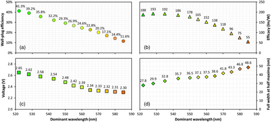
Figure 2: Dependence of (a) WPE, (b) efficacy, (c) voltage and (d) spectral full-width at half maximum (FWHM) on wavelength for InGaN-based LEDs on Si substrate from green to orange emission range.
The researchers have combined blue, cyan, green and yellow InGaN LEDs and red AlGaInP LEDs in a color-mixing module. With 20A/cm2 injection the color coordinates coincided with the ‘Planckian’ locus with 2941K correlated color temperature. The color-rendering indices were 97.5Ra (96.2R9). The efficacy was 121.3lm/W. The researchers report that the module is already being commercialized.
https://doi.org/10.1364/PRJ.7.000144
The author Mike Cooke is a freelance technology journalist who has worked in the semiconductor and advanced technology sectors since 1997.


