


- News
20 March 2019
EVG partners with NSI on wafer-level heterogeneous integration of GaAs-on-Si for RF front-end modules
EV Group of St Florian, Austria – a supplier of wafer bonding and lithography equipment for semiconductor, micro-electro-mechanical systems (MEMS) and nanotechnology applications – has partnered with Chinese specialty foundry Ningbo Semiconductor International Corp (NSI) to develop what is said to be the first process technology platform for wafer-level heterogeneous integration of gallium arsenide (GaAs) on silicon for use in RF front-end module (FEM) manufacturing – reckoned to be a key milestone in developing next-generation, high-performance, ultra-compact RF front-end chipsets needed for 4G and 5G smartphones and other handsets.
As a joint venture subsidiary of Semiconductor Manufacturing International Corp (SMIC) with China IC Investment Fund, Ningbo Economic Development Zone Industrial Investment Company Ltd and other IC investment funds, NSI develops technology platforms for high-voltage analog, radio frequency and optoelectronics applications. Developments support customers in IC design and product development for applications in smart home, industrial and automotive electronics, new generations of radio communications, AR/VR/MR, and other specialty systems.
As part of the strategic collaborative effort, EVG provided NSI with its temporary bonding/debonding (TB/DB), permanent bonding, mask alignment lithography and related special metrology equipment and process expertise, which NSI leveraged together with its proprietary micro wafer-level system integration (μWLSI) technology platform to produce the RF FEM products for a “leading RF front-end devices and system solution provider”.
“High-performance, ultra-compact RF front-end microsystem components are vital to the success of the 5G wireless terminal,” says NSI’s CEO Dr Herb Huang. “To support the customers and their RF front-end module products of the next generation of wireless terminals for meeting the stringent requirements of lower insertion loss, higher energy efficiency, ultra-miniaturization etc, it is necessary to provide more advanced wafer-level multi-chip heterogeneous integration process solutions for supporting and helping the customer meet the product standards and quickly ramp to volume production,” he adds. “We are pleased to have access to EV Group’s leading wafer bonding technology, lithography technology and expertise in heterogeneous integration.”
Wafer-level heterogeneous integration needed for 5G
As RF FEMs include key components such as power amplifiers (PAs), antenna switches and filters, the high-density 3D heterogeneous integration of materials with different properties, such as GaAs and silicon, is effective in enabling improved gain, linearity and power performance. At the same time, however, the migration to 5G broadband wireless technology is driving the need for wider multi-band PAs and more RF filters in the FEM, which in turn can drive up cost and footprint of the overall chipset package. Enabling heterogeneous system integration at the wafer level provides a cost-effective approach for achieving greater chipset density with minimal footprint increase, says EVG.
“5G is offering huge opportunity to the RF front-end industry,” comments Cédric Malaquin, technology and market analyst, RF Devices and Technology, at market research and strategy consulting company Yole Développement. “5G will completely redefine the interactions between the network and the modem. Indeed, new RF bands, sub-6GHz and mm-wave pose big challenges for the industry.” The mobile handset RF front-end market, along with the WiFi connectivity sector, is projected to rise at a compound annual growth rate (CAGR) of 14% to $35.2bn in 2023, according to last year’s report ‘5G’s Impact on RF Front-End Module and Connectivity for Cell Phones’ by Yole.
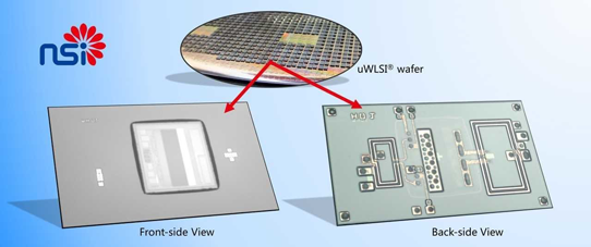
Picture: NSI’s proprietary μWLSI technology.
μWLSI is a middle-end-of-line technology platform for a unique wafer fabrication process developed by NSI for enabling heterogeneous multi-die-on-wafer system integration and wafer-level system testing while eliminating the need for bumping and flip-chip processes in typical system-in-package (SiP) practices. NSI developed the μWLSI technology platform specifically to address the surging need for high-density heterogeneous system integration of a variety of chipsets and microsystems through more wafer-level fabrication processing.
EVG says that its TB/DB systems play a key role in enabling the heterogeneous integration of compound semiconductors with silicon devices in a More-than-Moore approach. For example, TB/DB facilitates the reliable transfer and processing of very thin compound semiconductor, silicon and mold wafers, which can be integrated into higher-density vertical packages. Likewise, EVG’s mask alignment systems support wafer-level heterogeneous integration by enabling lithography patterning of carrier-mounted and warped substrates, which is essential for the μWLSI process.
“NSI is at the forefront in the development of specialty semiconductors for next-generation wireless and telecommunications technologies, such as 5G,” comments Swen Zhu, EVG’s general manager, China. “NSI has entrusted us once again to work with them to support their advanced manufacturing efforts - this time on their ground-breaking development in RF FEM platforms,” he adds. “The expertise that we have built up as a technology and market leader in wafer bonding and lithography process solutions will play an important role in our work with this leading foundry company.”
EVG is showcasing its latest wafer bonding and lithography solutions for heterogeneous integration and other applications in booth #2547 (Hall N2) at SEMICON China 2019 at the Shanghai International Expo (20-22 March).


