


- News
12 June 2019
Imec demonstrates optimized process flows for high-performance Ge-based devices
At the 2019 Symposia on VLSI Technology and Circuits in Kyoto, Japan (9-14 June), nanoelectronics research centre imec of Leuven, Belgium has reported improved performance for two types of germanium (Ge)-based device: both n-type FinFETs and p-type gate-all-around (GAA) devices.
For Ge n-type FinFETs, pre-gate stack process optimization dramatically improved reliability and performance, with 100% improvement in positive-bias temperature instability (PBTI) and improvement in the benchmark of transconductance (GmSAT) versus subthreshold slope (SSSAT). For the Ge-based p-type GAA device, excellent short-channel control and performance were achieved with an improved extension-less junction scheme. The results are said to confirm the potential of Ge-based CMOS transistors as high-performance solutions for the 3nm-and-beyond technology nodes.
Due to the higher intrinsic mobility of Ge compared to Si, Ge-based FinFET devices have emerged as non-disruptive performance boosters for future technology nodes. While Ge p-type FinFET devices have been studied extensively, the development of well-performing, reliable Ge n-type FinFET devices is lagging behind. Imec says that it has now proposed an optimized process flow for the gate stack, solving one of the major challenges for Ge n-type FinFET development.
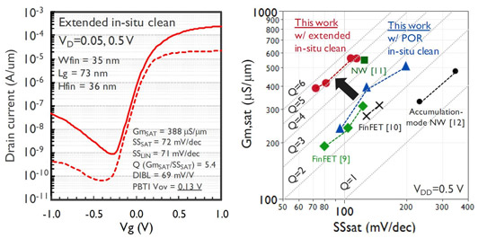
Graphic: Improved performance and reliability of Ge nFinFET device. (Left) Best ID-VG curves obtained from 35nm-wide Ge nFinFET with dummy gate oxide and extended in-situ clean. (Right) Extrinsic GmSAT versus SSSAT benchmark of n-channel Ge fin and nanowire FETs at VDD=0.5V.
Key to the successful gate-stack formation are an improved pre-cleaning and an optimized dummy gate oxide deposition and removal process, as part of a replacement metal-gate (RMG) process flow. Imec’s optimized process flow resulted in 100% improved positive-bias temperature instability (PBTI) and a 100% improvement in GmSAT versus SSSAT benchmark – a measure for the interface quality and electron mobility. “With our process flow, the oxide-free Ge channel surface can be prepared prior to the gate and efficiently protected from oxidation,” says logic program manager Naoto Horiguchi. “The paper describing these results was selected by the committee members of the VLSI Symposium as a highlight 2019 VLSI technology paper. It underlines the importance of our improved dummy gate oxide process for the formation of high-performance and reliable Ge n-type FinFETs.”
In a second paper, imec proposes an improved junction scheme to solve one of the major challenges for p-type strained Ge-based GAA devices, i.e. achieving good short-channel control while preserving transistor performance. A dramatic improvement in short-channel control – allowing gate-length scaling down to 25nm – was achieved by using an extension-less scheme, i.e. without dopant implantation in the ‘extension’ region next to the gate. To maintain the transistor’s performance, the extension-less scheme was combined with spacer thickness reduction, and with the implementation of highly boron-doped Ge or GeSn as the source/drain material. The optimized process flow resulted in a 55% improvement in the GmSAT versus SSSAT benchmark on Ge GAA devices compared with previous work. A short-channel (LG~25nm) device has also shown excellent Gm (Gm,lin=512µS/μm, GmSAT=2220µS/µm).
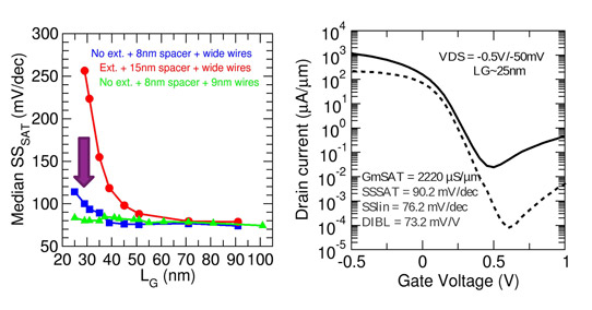
Graphic: (Left) Median SSSAT versus physical gate length for strained p-type Ge GAA devices with double nanowires. Significantly improved electrostatic control below LG=40nm. (Right) Best ID-VG characteristic of 9nm wires diameter Ge GAA with 25nm gate length by using extension-less scheme and scaled 8nm spacer. Reported data are normalized to total effective channel perimeter.
“Ge GAA devices have the potential to further extend gate-length scaling beyond what is possible with Ge-based FinFETs,” says Horiguchi. “They can be fabricated by using a process flow that is not so disruptive compared to FinFET processing,” he adds. “Much of the learnings we obtain from FinFET development can be transferred to GAA devices. By using our extension-less scheme, we have now demonstrated the feasibility of these Ge-based GAA devices for gate-length scaling down to 25nm, while preserving excellent performance.”
Imec demos first strained germanium FinFETs at IEDM
Imec demos first III-V FinFET devices monolithically integrated on 300mm silicon


