


- News
11 July 2019
Gallium nitride quantum well high-electron-mobility transistors
Cornell University in the USA has reported on what it claims is the first study of off-state breakdown in gallium nitride (GaN) quantum well high-electron-mobility transistors (QW-HEMTs) [Austin Hickman et al, IEEE Electron Device Letters, published online 14 June 2019]. The well was situated in aluminium nitride (AlN) barriers. The devices contrast with more conventional III-nitride transistor structures with a thick GaN layer, thin top AlGaN barrier and, sometimes, an AlGaN back barrier.
The researchers see the QW-HEMTs as having potential for high-power radio frequency applications. They explain: “GaN’s wide bandgap, large critical fields, high electron mobility, and excellent thermal conductivity enable low on-resistance and high breakdown voltages in GaN high-electron-mobility transistors.”
The researchers used plasma-assisted molecular beam epitaxy (MBE) to create strained GaN QW structures in unstrained AlN barriers on 6H polytype silicon carbide (SiC). The layer sequence was: 350nm AlN buffer, 30nm GaN channel, 4nm AlN barrier, and 2nm GaN cap passivation.
The channel consisted of a two-dimensional electron gas (2DEG) near the AlN/GaN top barrier interface, which forms due to contrast in the charge polarization effects in GaN and AlN. The electron density and mobility were measured at 2.9x10¹³/cm2 and 630cm2/V-s, respectively, using the Hall effect. Other reports of AlN/GaN/AlN 2DEG mobility have reached 700cm2/V-s.
The team comments: “Several factors may be playing a role in the mobility limitation, including the high electron concentration that may increase the electron effective mass, increased interface roughness scattering, and the possibility for a 2D hole gas (2DHG) at the GaN channel/AlN buffer interface.”
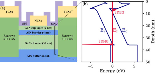
Figure 1: (a) Cross-sectional representation of processed QW HEMT, and (b) corresponding simulated energy band diagram.
The HEMT was fabricated in a gate-last process (Figure 1) with etching and MBE regrowth of the heavily doped n++-GaN ohmic source/drain contacts, mesa etching 20nm into the AlN buffer for electrical isolation, deposition of titanium/gold (Ti/Au) source/drain electrodes and nickel/gold (Ni/Au) gate, passivation with 40nm low-power plasma-enhanced chemical vapor deposition (PECVD) silicon nitride (SiN), and buffered oxide etch through the passivation for contact probing.
Transfer-length method and Hall measurements after fabrication indicated an increase in sheet resistance (510Ω/square, 50% greater than the as-grown value) and a reduction in electron mobility (410cm2/V-s). The electron concentration was 3x10¹³/cm2. The contact resistance of source/drain to the 2DEG was 0.13Ω-mm, described as “excellent” by the researchers. The increase in sheet resistance was likely due to surface damage, which could be avoided by altering the silicon dioxide deposited as a hard mask during fabrication.
The on/off current ratio was 104 – without passivation a value of 109 was achieved. The passivated device also achieved a peak transconductance of 0.6S/mm. “This is the highest transconductance reported for devices on the AlN/GaN/AlN heterostructure platform and shows their high promise,” according to the team.
The drain current reached 2.3A/mm with 1.3Ω-mm on-resistance. Under pulsed operation, the dispersion in current performance was around 15%. Frequency-dependent measurements in the range 0.05-40GHz gave cut-off (ft) and maximum oscillation (fmax) frequencies of 161GHz and 70GHz, respectively. The researchers comment: “Both ft and fmax values are records for HEMTs on the AlN platform. Further scaling of gate length and incorporation of a T-gate geometry are expected to dramatically increase ft and fmax for the QW HEMT.”
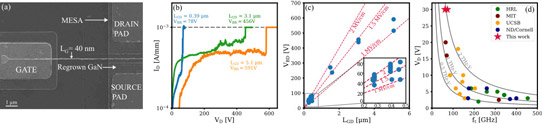
Figure 2: (a) Scanning electron microscope image of short-channel QW HEMT with 40nm gate length. (b) Hard breakdown for three HEMTs with varied gate-drain separations. (c) Breakdown voltage scaling as function of gate-drain separation from 0.27 to 5.1μm. (d) Johnson figure of merit benchmark plot comparing QW HEMT to state-of-the-art GaN HEMTs with submicron LGD and no field plate.
Breakdown (VBR) at 1mA/mm drain current density (ID) with the gate pinched off at less than -8V was 591V in a device with 5.1μm gate-drain distance (LGD, Figure 2). The average electric field at breakdown was 1.16MV/cm. All other devices also had average breakdown fields greater than 1MV/cm. The field increased to 2MV/cm for a 390nm gate-drain distance, giving a breakdown voltage of 78V. “This is among the largest breakdown voltages reported for a submicron channel nitride HEMT, demonstrating the potential of QW HEMTs for extremely high-power operation in RF applications,” the team reports.
The gate and drain currents were roughly similar during the breakdown measurements. “This indicates the off-state drain current and breakdown is dominated by gate-drain leakage and not avalanche or channel breakdown, and is far from the material limits,” the team explains. The researcher suggest that a refined SiN passivation focused on limiting gate leakage could improve breakdown performance.
Two devices with 80nm gate length and 460μm gate-drain distance demonstrated Johnson figures of merit (VDxft) of 2.2THz-V and 1.9THz-V with 30V drain bias (VD). The small-signals cut-offs were 73GHz and 62GHz, respectively. These are claimed to be among the highest reported.
QW-HEMTs GaN QW-HEMTs GaN SiC MBE
https://doi.org/10.1109/LED.2019.2923085
The author Mike Cooke is a freelance technology journalist who has worked in the semiconductor and advanced technology sectors since 1997.


