


- News
24 January 2019
Multi-channel tri-gate III-nitride high-electron-mobility transistors on silicon
Researchers based in Switzerland and China have fabricated tri-gate metal-oxide-semiconductor high-electron-mobility transistors with five III-nitride semiconductor channel levels, boosting electrostatic control and drive current [Jun Ma et al, Appl. Phys. Lett., vol113, p242102, 2018].
École Polytechnique Fédérale de Lausanne (EPFL) in Switzerland and Enkris Semiconductor Inc in China used a material structure consisting of five parallel layers of a 10nm aluminium gallium nitride (AlGaN) barrier, 1nm AlN spacer and 10nm GaN channel (Figure 1). The barrier was silicon doped at a partial level of 5x10¹⁸/cm3 to enhance conductivity.
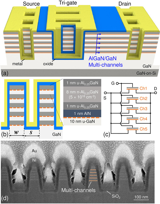
Figure 1: (a) Schematic of multi-channel tri-gate AlGaN/GaN MOSHEMT. (b) Cross-sectional schematic of tri-gate region. Inset: multi-channel heterostructure. (c) Equivalent circuit. (d) Cross-sectional scanning electron microscope image of tri-gate region, tilted by 52°.
Hall measurements on the five parallel thin two-dimensional electron gas (2DEG) channels gave the sheet resistance as 230Ω/square with 1.5x10¹³/cm2 carrier density and 1820cm2/V-s mobility (μ). The effective resistivity (ρeff) was 2.4mΩ-cm but with small total thickness (ttot). The team comments: “Small ρeff and high μ are crucial to reduce RON, and a thin ttot facilitates electrostatic gate control and device fabrication (the etching of high-aspect-ratio fins and the formation of electrodes around them can be challenging).”
The tri-gate structure was achieved with patterned inductively coupled etching to a depth of 200nm. The ohmic source/drain contacts consisted of annealed titanium/aluminium/titanium/nickel/gold. The gate stack was 25nm atomic layer deposition (ALD) silicon dioxide insulator and nickel/gold electrode.
One device had a gate length of 51μm: 50μm fin length +2x0.5μm extensions towards source and drain. Control of the channel current was affected by the fin width. In particular, with wide fins, control of the deeper channels was sluggish. This was shown by the transconductance exhibiting five peaks – one for each channel – when the width was greater than 200nm. The peaks merged at 40nm width. The 40nm device demonstrated a small negative threshold of -0.08V, improved subthreshold swing of 101mV/decade, and 29.5mS/mm peak transconductance.
Of course, reducing fin widths tends to reduce drain current in the on state. The multiple channels compensate for this somewhat. The maximum current decreased steadily as the fin width was reduced in single-channel devices, while for five channels the impact was only apparent for widths less than 200nm. With 100nm-wide fins, the single-channel current was reduced by 41% relative to a planar gate; the 5-channel reduction was only 12%.
The researchers explain that “the multi-channel structure mitigates greatly the electron-electron and sidewall scatterings in tri-gate (MOS)HEMTs.” The electrons in single-channel devices are tightly packed, increasing the rate of electron-electron collisions and hence resistance. Further resistance comes from more electrons hitting the fin sidewalls. Multi-channel structures reduce electron crowding in the separate channels.
A high-voltage MOSHEMT was produced with 10μm gate drain spacing, and 700nm-long, 100nm-wide fins. The spacing between the fins was 100nm, giving a fill factor of 50%. The gate metal extended 0.5μm towards the source and 1.3μm in the drain direction, giving a total length of 2.5μm.
Two single-channel reference devices were fabricated with similar dimensions: one with planar- and the other with tri-gate structures. The barrier layer in these reference devices was a typical 20nm of Al0.25Ga0.75N on GaN channel.
The multi-channel tri-gate devices showed reduced on resistance (Figure 2). Compared with the single-channel tri-gate reference, the on-resistance was almost half, and the maximum drain current increased more than three-fold. Normalized by the device width, the on-resistance was 6.0Ω-mm for the multi-channel MOSHEMT, compared with 11.2Ω-mm for the single-channel device. The multi-channel and single-channel maximum drain currents were 797mA/mm and 252mA/mm, respectively.
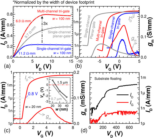
Figure 2: (a) Output characteristics at 5V gate potential (VG) and (b) transfer characteristics at 5V drain bias (VD), normalized by width of device footprint. (c) Transfer characteristics of multi-channel tri-gate transistors with 20nm fin width and 10% fill factor at 5V VD. Inset: threshold voltage (VTH, for 1μA/mm current) versus fin width (w) for two fin lengths (l).(d) Typical off-state breakdown characteristics of multi-channel tri-gate transistors measured with floating substrate.
The team comments: “These results are remarkable since they indicate that the multi-channel tri-gate technology can lower the conduction losses of the transistor for a given device footprint, or equivalently deliver a given current rating in a smaller device footprint, both of which are highly beneficial for efficient power transistors.”
Compared with the planar reference, the multi-channel MOSHEMT had 38% reduced on-resistance and 41% increased maximum drain current. This was despite the 50% fill factor of the fin structure, compared with the 100% of the planar setup.
The threshold voltage was made more positive by moving from the planar reference to the multi-channel fin MOSHEMT, going from -7.6V to -3.6V, respectively. The peak transconductance also increased 2.4-fold in the multi-channel device – 156.6mS/mm, compared with 66.1mS/mm. The on/off current ratio of the multi-channel MOSHEMT was ~1010.
Using a 20nm fin width (700nm length), the researchers achieved a positive threshold voltage of 0.82V a 1μA/mm. The off-current at 0V gate potential was 12pA/mm. Positive thresholds are desired for normally-off, enhancement-mode operation. The researchers attribute the positive threshold to the sidewall depletion effect. For longer 1.5μm fins, the sidewall depletion fin width was slightly increased to 24nm, likely due to increased strain relaxation relative to shorter fins.
Hard off-state breakdown came at 715V, while the gate leakage was still of order 0.2nA/mm at 700V drain bias.
https://doi.org/10.1063/1.5064407
The author Mike Cooke is a freelance technology journalist who has worked in the semiconductor and advanced technology sectors since 1997.


