


- News
1 February 2019
Octagonal cell topology for high-frequency silicon carbide transistors
Kijeong Han and BJ Baliga of North Carolina State University in the USA have developed 4H-polytype silicon carbide (4H-SiC) octagonal cell power metal-oxide-semiconductor field-effect transistors (MOSFETs) with reduced gate capacitance and charge, giving improved high-frequency figures of merit (HF-FOMs) over conventional linear-layout devices [IEEE Electron Device Letters, published online 21 December 2018].
The work represents the first “experimental demonstration of improved HF-FOMs for 4H-SiC power MOSFETs by using an octagonal-cell topology,” according to Han and Baliga. The devices were aimed at 1.2kV-rating applications.
The accumulation-mode channel (Accu) ‘OCTFET’ (Figure 1) used straight-edged structures, which can be defined more precisely in manufacturing than curves. However, simulations used to design the device used a circular approximation of the octagonal form to simplify the calculations.
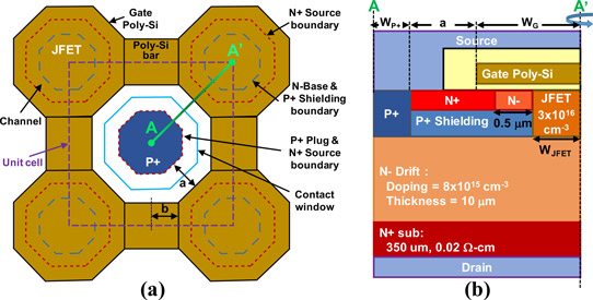
Figure 1: (a) OCTFET cell layout topology. (b) MOSFET cell cross section at A-A’.
The design sought to reduce capacitance and charge on the gate to enable faster switching speeds and lower power consumption. There was some trade-off in increased specific on-resistance for the reduced capacitance/charge.
Accu OCFET device designs were sent to commercial foundry X-FAB in Texas, USA, for fabrication on 6-inch-diameter 4H-SiC silicon-face (0001) wafers. The junction FET region width (WJFET) varied between 0.9μm and 1.5μm (O_J0.9-1.5). The channel-gate distance (a) was also 1.1μm. The half-lengths of the bars connecting the four component JFETs (b) was 1.1μm. A ‘compact’ version with smaller 0.55μm ‘b’ value and WJFET of 1.1μm was also produced (O_J1.1_C).
The n- and p-type regions were created using ion implantation of nitrogen and aluminium, respectively. The resultant doping was activated using 1650°C annealing with a carbon cap. Dry oxidation at 1175°C was used for the 50nm gate insulator. The insulator interface was also annealed in nitric oxide gas. The gate electrode was 500nm n-type polysilicon. Annealed nickel silicide was used for the ohmic source-drain contacts. The source and gate pads were aluminium. A solderable metal stack was applied to the back-side drain contact.
Devices with wider JFET regions had lower specific on-resistance (Ron,sp) at gate potential of 20V and drain current 10A (Table 1). The values include the substrate resistance (~0.7mΩ-cm2). The compact device also performed well on this metric. A linear-layout comparison device with WJFET of 0.7μm had even lower specific on-resistance, due to a greater channel density. The results obtained were in line with the researchers’ simulations.
Table 1: Summary of experimental results for OCTFETs and conventional linear MOSFET.
| linear_J0.7 | O_J0.9 | O_J1.1 | O_J1.3 | O_J1.5 | O_J1.1_C | |
| BV | 1628V | 1639V | 1605V | 1630V | 1607V | 1605V |
| Vth | 1.96V | 2.04V | 2.02V | 2.06V | 2.12V | 2.12V |
| Ron,sp | 5.61mΩ-cm2 | 25.52mΩ-cm2 | 12.82mΩ-cm2 | 9.72mΩ-cm2 | 8.38mΩ-cm2 | 8.47mΩ-cm2 |
| Cgd,sp | 106pF/cm2 | 21pF/cm2 | 28pF/cm2 | 53pF/cm2 | 72pF/cm2 | 34pF/cm2 |
| Qgd,sp | 311nC/cm2 | 67nC/cm2 | 113nC/cm2 | 160nC/cm2 | 233nC/cm2 | 144nC/cm2 |
| RxC | 595mΩ-pF | 536mΩ-pF | 359mΩ-pF | 515mΩ-pF | 603mΩ-pF | 288mΩ-pF |
| RxQ | 1745mΩ-nC | 1710mΩ-nC | 1449mΩ-nC | 1555mΩ-nC | 1953mΩ-nC | 1220mΩ-nC |
The gate-drain capacitance (Cgd,sp) and charge storage (Qgd,sp) were measured at drain biases of 1000V and 800V, respectively. In this case, the smaller-WJFET devices with reduced junction area performed best, while the linear comparison was even worse than the larger OCFETs.
The breakdown voltages (BVs) of all the devices were greater than 1600V, far exceeding the 1.2kV target rating. Threshold voltage (Vth) with 0.1V drain bias for 1mA drain current were around 2V.
The HF-FOMs were based on the products of the specific on-resistance and capacitance/charge (RxC/RxQ), showing the lowest values for the compact device. The linear layout had 2.1x and 1.4x worse capacitance and charge HF-FOMs, respectively. Among the standard devices, the 1.1μm OCFET was optimal, also beating the linear layout.
https://doi.org/10.1109/LED.2018.2889221
The author Mike Cooke is a freelance technology journalist who has worked in the semiconductor and advanced technology sectors since 1997.


