


- News
21 February 2019
LayTec launches EpiX modular wafer mapping station for compound semiconductor R&D
In-situ metrology system maker LayTec AG of Berlin, Germany has launched the EpiX wafer mapping station for compound semiconductor R&D.
Currently, there is an ongoing boom in metal-organic chemical vapor deposition (MOCVD)-grown III-V lasers, with a corresponding resurgence in related material research, notes the firm. LayTec already supports this with in-situ metrology products such as EpiTT VCSEL or EpiTT FaceT, and EpiX is the next new product. The first EpiX station was installed at a customer site in mid-2018, and combines white light reflectance with photoluminescence (PL) measurements, allowing comprehensive 2D analysis over a wide spectral range (400-1700nm).
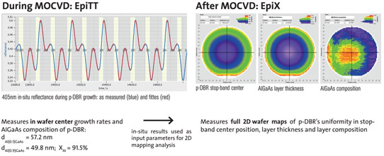
Up to four PL excitation wavelengths can be combined with an optional eye-safe plug-in interface for a user’s additional external excitation lasers. Integrated software provides full data analysis, including automated detection of vertical-cavity surface-emitting laser (VCSEL) optical parameters (cavity-dip, stop-band position), single-layer and multiple-layer thickness fits, film composition and multiple-peak analysis. Moreover, users can benefit from a sample’s statistics and pass/fail classification at both the wafer level and die level.
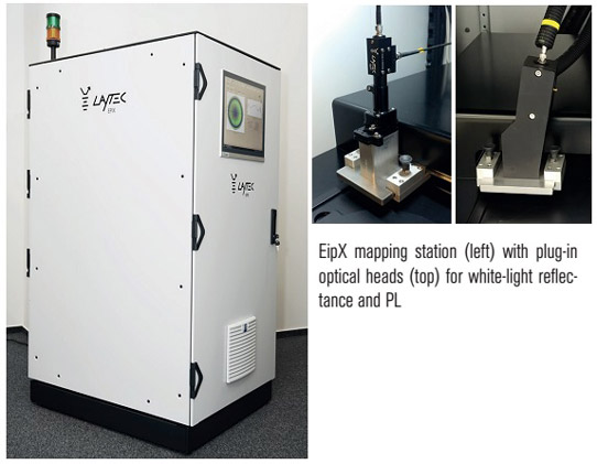
The basic design feature of EpiX mapping stations is modularity and customizability in hardware and software. This is key for users that regularly adjust their research projects to new materials and the latest nano-science concepts, says LayTec. EpiX is hence designed as a long-lasting workhorse with multiple upgrade options: more optical heads (wafer bow, reflectance-anisotropy, sheet resistance, wafer thickness, optical transmission), extended wavelength range, software interfaces (e.g. for user-owned spectral analysis libraries) and for using in-situ data measured during epitaxy at the center of the wafer as a starting point for post-epi 2D mapping analysis.


