


- News
19 February 2019
Monolithic indium arsenide antimonide on silicon mid-infrared photodetector
Lancaster University and University of Warwick in the UK have monolithically integrated indium arsenide antimonide (InAsSb) mid-infrared (MIR) photodetectors on silicon [Evangelia Delli et al, ACS Photonics, web publication 16 January 2019]. The devices used a ‘type-II’ structure with an aluminium gallium arsenide antimonide Al0.9Ga0.1As0.1Sb0.9 electron-blocking barrier sandwiched between n-type InAs/InAsSb superlattices (SLs) to give an ‘nBn’ band structure that presents a barrier to electrons and a well to holes.
The researchers see opportunities for cost-effective silicon photonics and thermoelectrically cooled detection systems on silicon for the 3-5μm-wavelength MIR spectral range. Low-cost ultra-compact systems in the forms of large-area focal plane arrays and MIR integrated photonic circuits would find ready deployment in gas sensing, defense and medical diagnostics.
The usual materials used in the MIR range are mercury cadmium telluride (HdCdTe) alloys. The resulting devices are expensive to produce and need cryogenic cooling to reduce dark current.
The team explains the advantage of nBn photodetection: “These structures (often referred to as nBn) employ a wide-bandgap barrier layer positioned between narrow-bandgap absorption and contact layers which blocks the flow of majority carriers (electrons), but not that of minority carriers (holes). A small applied bias falls almost completely across the barrier separating the photo-generated carriers. This almost entirely eliminates the electric field in the narrow-gap material, which greatly suppresses the junction-related Shockley-Read-Hall (SRH) dark current, resulting in significantly higher operating temperatures compared to conventional p-i-n photodiodes.”
A number of epitaxial techniques were used to achieve low defect densities in the MIR-absorbing material. In addition, defects in InAsSb structures tend to have energy levels above the conduction band, rather than in the gap between the valence and conduction bands. This reduces the SRH dark current, since the mechanism flows through mid-gap levels.
Material growth began with a 17-monolayer AlSb nucleation grown by 490°C solid-source molecular beam epitaxy (SS-MBE) on 4°-miscut silicon (100) wafers (Figure 1). The nucleation included an optimized array of 90° interfacial misfit dislocations to encourage lateral rather than vertical propagation of defects. The spacing of the misfits was around 3.35nm.
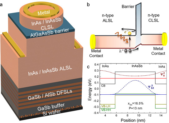
Figure 1: (a) Schematic of InAs/InAsSb type-II SL nBn structure grown on top of GaSb/AlSb/Si buffer, using AlSb/GaSb dislocation filters. (b) Device bandgap structure with barrier blocking electron flow. (c) Calculated InAs/InAsSb SL bandstructure with first electron and hole energy levels and carrier density (Ψ2).
The 2μm GaSb buffer was grown in two temperature steps at 490°C (1.5μm) and 515°C (0.5μm). The threading dislocations arising from the III-V/Si hetero-epitaxy were confined mainly to the first 700nm of the GaSb buffer. The buffer was also free of anti-phase domains.
Five sets of strained AlSb/GaSb dislocation-filter superlattices (DFSLs) further improved the material quality of the device layers. Each superlattice set consisted of five repeats of 10nm/10nm GaSb/AlSb. The sets were separated by 300nm GaSb spacers. After filtering, the threading dislocation density was 3x10⁷/cm2.
The absorption-layer superlattice (ALSL) and contact-layer superlattice (CLSL) were 4μm and 400nm thick, respectively. They were separated by an Al0.9Ga0.1As0.1Sb0.9 electron-blocking barrier with large conduction and small valence band offsets with the surrounding material. This enabled hole but not electron flow. The superlattice design consisted of 5.8nm/7.2nm InAs/InAs0.835Sb0.165 pairs – 320-periods in the ALSL and 30-periods in the CLSL. The growth temperature was 430°C. Tellurium was used as n-type dopant.
Wet etching was used to create the mesas for the photodiode device. The metal contacts were titanium/gold. Under 100mV reverse bias, the dark current was 8.65x10⁻¹A/cm2 at room temperature, decreasing to 1.2x10⁻³A/cm2 at 160K. While these values are lower than previously reported for Sb-based devices on silicon, HgCdTe devices typically have dark currents two orders of magnitude lower than the Lancaster/Warwick photodiode.
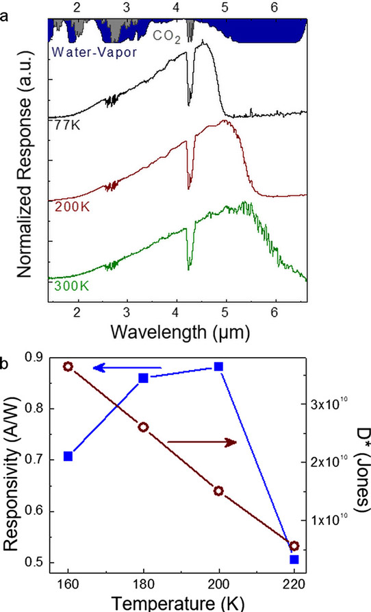
Figure 2: (a) Normalized spectral response curves for detector at different temperatures (CO2 absorption shown in gray, water vapor absorption in blue). (b) Total spectral responsivity and specific detectivity, D*, values measured as function of temperature in 3.7-4.9μm spectral band.
The spectral response under 100mV reverse bias had a 50% cut-off at 5.40μm at 200K, rising to 5.86μm at 300K/room temperature (Figure 2). The responsivity in the spectral range 3.7-4.9μm to an 823K blackbody source was 0.88A/W, representing a 25.6% external efficiency. At the slightly higher photodiode temperature of 220K, the response fell to 0.5A/W.
Specific detectivity (D*) calculations, which take into account thermal and shot noise limitations on performance, gave values of 3.65x10¹⁰Jones at 160K and 1.5x10¹⁰Jones at 200K. The researchers comment: “These results are higher than bulk InSb detectors grown previously on silicon and that of InAs/GaSb SLs grown on GaAs. This can be attributed to the improved structural quality of the GaSb/Si buffer layers, and the reduced defect sensitivity provided by the InAs/InAsSb SL nBn design. However, they are about an order of magnitude lower than state-of-the-art InAs/InAsSb SL nBn photodetectors integrated on native GaSb substrate reported recently by Nasa JPL.”
The team suggests that improved performance could come from back-side illumination or the use of anti-reflective coatings. As always, improved material quality with further reduced threading dislocation density would also help achieve lower dark currents.
InAsSb Mid-infrared photodetectors AlGaAsSb electron-blocking barrier nBn band
https://doi.org/10.1021/acsphotonics.8b01550
The author Mike Cooke is a freelance technology journalist who has worked in the semiconductor and advanced technology sectors since 1997.


