


- News
30 April 2019
SMI delivers two 2D metal dichalcogenide systems
Structured Materials Industries Inc (SMI) of Piscataway, NJ, USA – which provides chemical vapor deposition (CVD) systems, components, materials and process development services – has delivered metal-organic chemical vapor deposition (MOCVD) research systems to two US universities. The two MOCVD systems are part of the NanoV CVD and NanoH CVD series and are configured primarily for the growth of 2D transition metal dichalcogenide materials, of which a variety are under investigation (for optoelectronic devices, solar cells, photo-detectors, light-emitting diodes and photo-transistors) including MoS2, WS2, MoSe2 and WSe2.
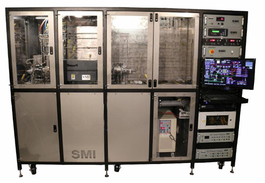
Picture: An SMI-designed and -fabricated dual-reactor Nano CVD and NanoH CVD system.
One system features a dual-reactor arrangement of a NanoV CVD and a NanoH CVD. The east-coast research professor’s group focuses on integrating, assembling and characterizing atomic-scale materials into electronic and photonic devices for various applications. The vertical and horizontal reactors allow for significantly different process phase spaces to be investigated in optimizing 2D materials. This is the second such tool for this professor.
The second tool is a single NanoH CVD research system for a professor at a California university. Similarly, this professor had used an SMI-built system as a post-doc at his previous university. His group specializes in areas such as the systematic design of oxide, carbide and sulfide materials for materials synthesis of multi-dimensional device architectures in applications such as energy conversion and storage.
“There is always a need for custom versatile tools that can robustly and reproducibly produce advanced materials that are at the forefront of research and development efforts - such as, in the present case, high-quality 2D materials,” says president Dr Gary S. Tompa. “Also important are the size scalability of the tools. The standard capabilities of these tools - such as the multi-zoned temperature-controlled furnace or field-recalibratable mass flow controllers or a versatile researcher-oriented control system such as SMI’s SmartCVD PLC control system - allow for easily switching amongst the most promising growth materials, processes, and tool configurations,” he adds. “We designed these specific tools to be both flexible and to address the exacting needs of growing the latest 2D materials that are associated with forming stable monolayer, single-unit-cell-thick films to easily produce materials for advanced device research and prototype manufacturing.


