


- News
5 April 2019
Non-polar GaN-based VCSEL diode with nanoporous distributed Bragg reflector
The University of New Mexico and Sandia National Laboratories in the USA claim the first electrically injected non-polar m-plane gallium nitride (GaN)-based vertical-cavity surface-emitting lasers (VCSELs) with conducting lattice-matched nanoporous bottom distributed Bragg reflectors (DBRs, Figure 1) [Saadat M. Mishkat-Ul-Masabih et al, Appl. Phys. Express, vol12, p036504, 2019]. Optically-pumped m-plane GaN VCSELs with nanoporous DBRs have been previously reported by the group, and others have presented c-plane devices.
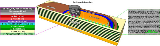
Figure 1: Cross-sectional schematic of m-plane nanoporous VCSEL and scanning electron micrograph of bottom nanoporous DBR.
GaN-based VCSELs are seen as having opportunities in data storage, laser printing, solid-state lighting, optical communications, sensing and display technologies. Longer-wavelength arsenide-based VCSELs typically have optically confining DBR structures that are also conducting. These DBRs are constructed from superlattices of semiconductor material with significantly different refractive index.
Refractive index contrast is more difficult to achieve in the III-nitride class of compound semiconductor alloys. Instead, non-conducting dielectric DBRs are typically used, making for more complex processing and fabrication of contact structures.
The epitaxial structure was grown on non-polar m-plane freestanding GaN substrates from Mitsubishi Chemical Corp, processed using metal-organic chemical vapor deposition (MOCVD). The active light-emitting region consisted of six indium gallium nitride (InGaN) quantum wells (QWs). Electron leakage into the p-type region was blocked by an aluminium gallium nitride (AlGaN) electron-blocking layer (EBL) barrier.
Mesa etching with inductively coupled plasma exposed the n+-GaN contact layer. A titanium/gold mask was used to define the current aperture that was then created by aluminium ion implantation at Leonard Kroko Inc. The implant mask was removed and a second mesa etched to a depth of 400nm was followed by blanket deposition of 150nm silicon dioxide protection of the epitaxial structure during DBR porosification.
Deep trenches were then etched in the c-direction to expose the bottom of the DBR sidewalls. An electro-chemical process selectively etched the n+-GaN layers of the bottom DBR structure to porosify the layer, reducing its refractive index. The DBR consisted of 16 pairs of 41nm/60nm undoped-/n+-doped GaN layers. The refractive index difference of the resulting layers was about 0.83.
The blanket silicon dioxide was removed and silicon nitride passivation applied to the active region sidewalls of the first mesa. The top contact structure included 50nm annealed transparent indium tin oxide (ITO) conductor. The metal contacts consisted of titanium/gold and titanium/aluminium/nickel/gold, respectively, for the p- and n-electrodes. The device was completed with a dielectric DBR constructed from quarter-wavelength pairs of silicon dioxide and silicon nitride (SiO2/SiNx) on a silicon nitride cavity spacer. The optical thickness of the cavity was designed to be eight wavelengths.
The team reports: “The layer thicknesses were designed to ensure that the active region of the device aligned with a peak and that the ITO aligned with a null of the standing-wave profile in the cavity to maximize gain and minimize optical loss.”
Pulsed measurements of 50ns width and 0.05% duty cycle were used to characterize the devices (Figure 2). Pulsed operation avoids self-heating that results in performance degradation. The threshold current density of a device with 20μm-diameter aperture was ~20kA/cm2. The corresponding voltage was 9.6V. The top DBR had a reflectivity of 99.7%. From the fraction of light emitted from the top and bottom of the device, the researchers estimated the bottom DBR’s reflectivity to be 99.9%. The maximum output power was around 1.5mW - “higher than any previously reported m-plane GaN-based VCSEL,” according to the team.
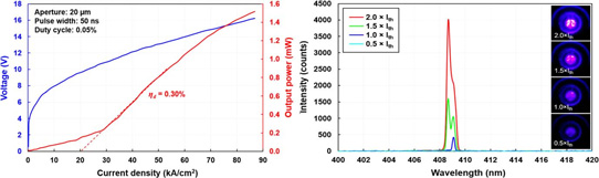
Figure 2: (a) Light output power-current density-voltage plot of 20μm-diameter nanoporous VCSEL under pulsed operation. (b) Emission spectrum under various pump currents and corresponding near-field images of aperture region.
At twice the threshold current injection the longitudinal-mode peak was at 408.7nm with a full-width at half-maximum (FWHM) of ~0.6nm. A secondary peak was seen at 409.1nm, but this is not thought to be from a higher-order mode since the expected spacing based on the cavity length was expected to be around 25.5nm. The researchers comment: “Our previous results indicate that non-uniformities in the optical cavity length due to localized changes in the effective refractive index of the nanoporous layers can lead to locally different single-longitudinal modes with same mode number but different wavelengths, which could result in multiple peaks within the lasing spectrum.”
Lasing filaments (‘spots’, as seen in near-field images, with different wavelength emissions) are commonly observed in III-nitride VCSELs. Apart from filamentary non-uniformities, the researchers also saw a discrete divide across the aperture for the emission at twice the threshold. This was seen as being due to “the intersection of the nanopore etching fronts from the positive and negative a-directions forming a break in the aperture”. The team hopes that moving the location of the aperture or pore etching from the c-direction could solve this issue.
The polarization of the light was around 94% with the maximum intensity measured when the polarizer angle was perpendicular to the [0001] c-direction – i.e. the polarization was along the [1-210] a-direction.
In temperature-dependent measurements up to 333K, the characteristic temperature of the threshold current (T0) was high at 357K. The researchers hope that reduced thresholds will result from the use of a tunnel junction rather than ITO contact with the p-GaN hole injector in future devices.
VCSEL GaN MOCVD GaN substrate InGaN AlGaN
https://doi.org/10.7567/1882-0786/ab0576
The author Mike Cooke is a freelance technology journalist who has worked in the semiconductor and advanced technology sectors since 1997.


