


- News
27 September 2018
Thin gallium nitride on silicon carbide high-power and high-frequency electronics
Researchers based in Sweden have developed thinner III-nitride structures on silicon carbide (SiC) with a view to high-power and high-frequency thin high-electron-mobility transistors (T-HEMTs) and other devices [Jr-Tai Chen et al, Appl. Phys. Lett., vol113, p041605, 2018]. Rather than having a ~1-2μm-thick gallium nitride (GaN) buffer layer, the new structure uses a high-quality 60nm grain-boundary-free aluminium nitride (AlN) nucleation layer to avoid extended defects over large areas (Figure 1). The nucleation layer allows high-quality GaN to be grown within 0.2μm.
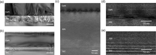
Figure 1: Cross-sectional transmission electron micrograph (TEM) images along the [11-20] direction at the GaN/AlN/SiC interface using (a) conventional and (b) low-TBR AlN nucleation. (c) High-magnification image of GaN/low-TBR AlN NL/SiC. (d) High-resolution image at the interface of the GaN/low-TBR AlN NL. (e) High-resolution image at the interface of the low-TBR AlN NL/SiC. Scale bar is 100nm in (a) and (b).
The normally thick buffer layers are used to transition and reduce defects arising from the 3.5% lattice mismatch between GaN and SiC – the mismatch is much higher for other substrates such as sapphire and silicon. These thick layers create problems for high-power and high-frequency devices. These layers are often doped with carbon or iron to increase resistance with the aim of confining current flow to the channel region, avoiding leakage effects from parasitic conduction. The doping creates charge-trapping states that can cause their own negative impacts on performance such as current collapse in radio-frequency operation.
Thinner devices should also have lower thermal resistance, improving thermal management. The team from SweGaN AB, Chalmers University of Technology, and Linkoping University, comments: “Structural defects like voids and dislocations generated at the interfaces of GaN/AlN/SiC introduce a thermal boundary resistance (TBR) that results in an additional 30-40% channel temperature rise in HEMTs.”
The reduced amount of expensive materials needed is a further attraction of the work. The researchers estimate a 90% reduction in raw materials including precursors and gases, along with reduced processing cost from the decreased growth time needed.
The new AlN nucleation process avoids the usual grain-like morphology that tends to result in column-like growth where defects are carried up into the overlying GaN. The usual graininess is due to the low mobility of aluminium atoms on the growth surface.
The III-nitride material was grown on silicon-face 4H silicon carbide. Hot-wall metal-organic chemical vapor deposition (MOCVD) was used to create epitaxial structures with 60nm AlN nucleation, a 200nm GaN channel, an AlN interlayer of up to 1.5nm, a 10-14nm AlGaN barrier (~30% Al), and a 2nm GaN cap. The 60nm AlN was produced using a low thermal-boundary-resistance (low-TBR) technique enabled by the hot-wall growth.
Despite the thinness of the structure, threading dislocations densities in the low 108/cm2 range was estimated, “two orders of magnitude less than that of the typical GaN layers with the same thickness,” according to the researchers. Contactless Hall measurements on a structure with a 2nm GaN cap and a 14nm Al0.29Ga0.71N barrier gave a 9.8x10¹²/cm2 two-dimensional electron gas (2DEG) density and a 2050cm2/V-s mobility. The sheet resistance was 315Ω/square.
Test T-HEMTs were produced on material with a 2nm GaN cap, a 10nm Al0.3Ga0.7N barrier and a 1nm AlN interlayer. Tantalum-based contacts were used for the source/drain, giving a contact resistance of 0.3Ω-mm.
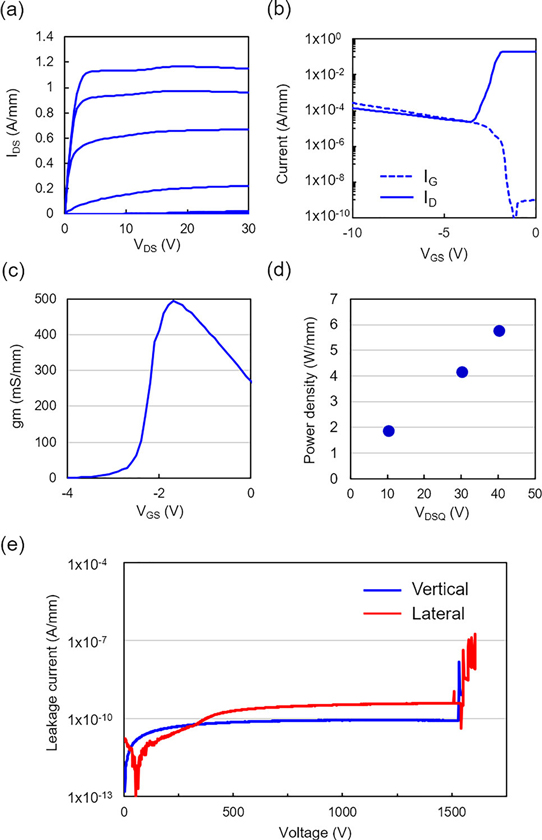
Figure 2: (a) DC drain current-voltage (IDS-VDS) characteristics, (b) transfer characteristics and gate and drain current at 10V drain bias (VDS) as a function of gate voltage (VGS), (c) transconductance (gm) as a function of gate potential, and (d) radio-frequency output power density as a function of VDSQ of T-HEMT. (e) Vertical and lateral breakdown characteristics of heterostructure without top active layers.
The device achieved a high on-current density of 1.1A/mm with low normalized on-resistance of 1.3Ω-mm (Figure 2). The saturation current was maintained up to 30V drain bias. With 10V drain bias, the pinch-off was sharp, with transconductance reaching 500mS/mm. The subthreshold swing depended on gate length: 250mV/decade for 0.1μm and 130mV/decade for 0.2μm. The breakdown voltages were 70V and 140V for the 0.1μm and 0.2μm gates, respectively.
The researchers comment: “The linear relationship between the breakdown voltage and the gate length suggests that the breakdown was taking place laterally due to the limited dimension of the gate length and the gate-to-drain spacing.”
The gate-drain spacing was 2μm, far short of the usual 10-20μm normally used in GaN HEMTs aimed at power performance. Also, conventional GaN power HEMTs have micron-scaled gate lengths.
Load-pull measurements at 30GHz gave a peak radio-frequency power density of 5.8W/mm at 40V drain-to-source quiescent bias (VDSQ).
Breakdown measurements on an epitaxial stack without the upper AlN/AlGaN layers gave breakdown voltages up to 1.5kV in both lateral and vertical directions. The team comments: “In both cases, the breakdown was due to the bad delineation of the contacts. Therefore, the real breakdown voltage of the stack is expected to be higher. In other words, the breakdown has been limited by the surface and it confirms that there are no interface carriers.”
https://doi.org/10.1063/1.5042049
The author Mike Cooke is a freelance technology journalist who has worked in the semiconductor and advanced technology sectors since 1997.


