


- News
13 September 2018
Magnetic sensing with gallium nitride high-electron-mobility transistors
Researchers at Swansea University in the UK and the University of Nis in Serbia claim the first fabrication of gallium nitride (GaN) magnetic high-electron-mobility transistors (MagHEMTs) [S Faramehr et al, Semicond. Sci. Technol., vol33, p095015, 2018].
The devices featured a split drain (Figure 1) that allowed the deviation of electron paths due to interaction with magnetic fields to be assessed. The relative sensitivity of such devices is given by the current difference between the drain terminals relative to the total drain current over the magnetic field in Teslas (T).
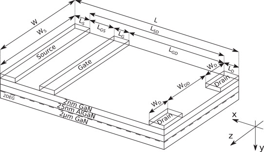
Figure 1: GaN MagHEMT (split-current sensor) schematic showing geometrical parameters used for relative sensitivity optimization.
Magnetic sensors are widely used for control in engineering systems covering aeronautical, automotive and industrial applications.
The devices were fabricated on HEMT heteroepitaxial structures with Al0.25Ga0.75N barrier layer. Step-graded AlGaN was used to transition from the silicon substrate. The length (L) and width (W) of the device were 35μm and 20μm, respectively. The lengths of the source (LS), and drain (LD) were both 5.5μm. The gate length (LG) was 1.0μm. The gate-source distance (L GS) was 1μm. The widths of the two drain contacts (WD) were 7.5μm each. The device was passivated with 10nm silicon nitride.
With the gate at zero and the drain bias at 0.5V, the sensitivity was found to be 11.98%/T – higher than previously reported values for silicon dual-drain split-current magnetic sensors.
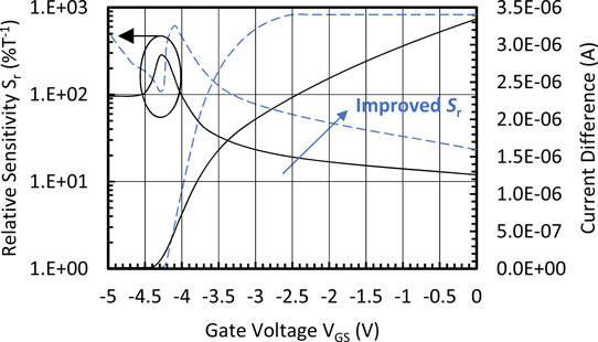
Figure 2: Simulated relative sensitivity (dash) and current difference (dash) of optimized GaN MagHEMT against simulated original GaN MagHEMT.
The researchers used the experimental results to calibrate a series of simulations aimed at optimizing performance. The model suggested that improved sensitivity of 23.29%/T, at zero gate potential and 0.5V drain bias, could be achieved in a device with altered parameters - L=65μm, W=20μm, LS =5.5μm, W S =5.0μm, WDD=5μm, L G =5.0μm and LGD=10μm (Figure 2).
The important changes seem to be a much longer total length of 65μm and reduced source width of 5μm. The reduced source contact decreases the total current flow and increases sensitivity to current deflection effects. The longer length also increases source to drain resistance, again reducing total current. The simulations also suggest an order-of-magnitude enhanced sensitivity at around -4V gate potential.
The researchers further studied the simulations at a raised temperature of up to 500K, showing “promising operation of GaN magnetic sensors under harsh environments”. However, there was a decrease in sensitivity to 4.91%/T for the original device structure.
https://doi.org/10.1088/1361-6641/aad58f
The author Mike Cooke is a freelance technology journalist who has worked in the semiconductor and advanced technology sectors since 1997.


