


- News
19 October 2018
Zhejiang University reports first current-collapse-free vertical GaN power rectifier
© Semiconductor Today Magazine / Juno PublishiPicture: Disco’s DAL7440 KABRA laser saw.
China’s Zhejiang University (ZJU) has reported what is claimed to be the first vertical gallium nitride on gallium nitride (GaN-on-GaN) power rectifier that is free from current collapse (i.e. has no dynamic ON-resistance degradation), even at only 200ns after switching from high reverse stress bias up to 500V, outperforming the state-of-the-art lateral gallium nitride on silicon (GaN-on-Si) devices. With the dynamic ON-resistance quantitatively evaluated under various switching conditions using a high-speed double pulse test circuit, the current-collapse-free performance has been experimentally verified in a vertical GaN power rectifier for the first time (‘Current-Collapse-Free and Fast Reverse Recovery Performance in Vertical GaN-on-GaN Schottky Barrier Diode’ by Shaowen Han, Shu Yang, Rui Li et al; IEEE Transactions on Power Electronics; DOI: 10.1109/TPEL.2018.2876444).
Dynamic ON-resistance degradation has been regarded as the primary challenge in conventional lateral GaN-on-Si devices, the root causes of which include: (1) surface trapping that can easily degrade the two-dimensional electron gas (2DEG) conductivity at a short distance from the III-nitride surface; and (2) a carbon-doped semi-insulating buffer stack containing deep-level traps that can generate negative space charges and partially deplete the 2DEG.
By comparison, featuring a vertical current flow and high-quality homo-epitaxial GaN drift layer with well controlled background/compensation doping, the vertical GaN-on-GaN device can fundamentally overcome the grand challenge of dynamic ON-resistance degradation.
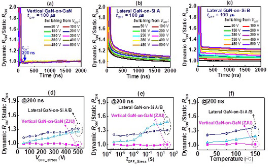
Figure 1: Time-resolved dynamic RON/static RON of (a) a vertical GaN-on-GaN Schottky barrier diode developed by ZJU, (b) a lateral GaN-on-Si commercial device A and (c) a lateral GaN-on-Si commercial device B with OFF-state time (tOFF_Stress) of 100μs and OFF-state bias (VOFF_Stress) increasing from 50V to 500V. Also shown are the extracted dynamic R ON/static RON of the three types of GaN devices at 200ns after switching from (d) various V OFF_Stress up to 500V, (e) various t OFF_Stress up to 100s, and (f) various temperature up to 150°C.
The dynamic ON-resistance has been quantitatively evaluated using the double pulse tester with a clamping circuit under different switching conditions, including: (1) OFF-state stress bias up to 500V, (2) OFF-state stress time within 10-6~102s, (3) high temperature up to 150°C, and (4) different load current levels. Under all the test conditions, the vertical GaN-on-GaN rectifier is free from dynamic ON-resistance degradation at only ~200ns after switching from the OFF-state, outperforming state-of-the-art commercial lateral GaN-on-Si devices and showing great potential for high-frequency applications, reckon the researchers.
https://ieeexplore.ieee.org/document/8493547


