


- News
9 October 2018
Silicon monoxide gate dielectric for gallium nitride transistors
Researchers based in China and the UK have explored thermally evaporated silicon monoxide (SiO) as a gate dielectric for gallium nitride (GaN) metal-oxide-semiconductor high-electron-mobility transistors (MOS-HEMTs) [Gengchang Zhu et al, Semicond. Sci. Technol., vol33, p095023, 2018].
The hope of the team from Shandong University and University of Manchester was that improved interfaces would reduce performance impacts from charge trapping states and so on. Dielectrics are often deposited using interface-damaging processes involving ion bombardment and reactive gases, often at high temperature, that are avoided with thermal evaporation.
GaN transistors are being developed for high frequency and high power handling for radio-frequency amplification, and power-switched power supplies and AC/DC, DC/AC conversion. The electronic properties that make GaN suitable for these applications include high breakdown field strength, high electron velocity, and thermal stability.
There are some barriers to progress towards commercial application such as gate leakage and current collapse when moving from DC to switched operation. Gate leakage is suppressed by inserting insulating dielectrics between the metal gate and semiconductor material. Current collapse is connected with charge-trapping states that introduce delay and hysteresis effects in performance.
The III-N heterostructure with aluminium gallium nitride (AlGaN) barrier layer consisted of 25nm/1nm/1.8μm Al0.22Ga0.78N/AlN/GaN grown by metal-organic chemical vapor deposition (MOCVD) on 2-inch 6H silicon carbide (SiC) with 100nm AlN nucleation. The GaN buffer layer was doped to be semi-insulating.
The material was used to fabricate mesa-isolated MES-HEMTs and MOS-HEMTs with titanium/aluminium/nickel/gold ohmic source-drain electrodes. For the MES-HEMT, the gate stack was nickel/gold. The MOS-HEMT included SiO in the gate stack from 99.99%-pure powder thermally evaporated from a tungsten boat and deposited at room temperature on the AlGaN barrier surface with a 0.55nm root-mean-square roughness for a 30nm layer, according to atomic force microscopy.
The devices featured a 2μmx100μm gate (width)x(length). The source-drain and gate-drain spacings were 14μm and 6μm, respectively.
One effect of the SiO gate insulation was to increase the maximum drain current to 452mA/mm for 30nm thickness, compared with 317mA/mm for the MES-HEMT (‘0nm’ SiO). The researchers suggest that the improved current may be due to the suppression of surface trapping effects by SiO passivation and/or passivation induced stress in the AlGaN layer.
Another related effect is an increase in carrier density in the channel region to 1.21x10¹³/cm2 from 8.1x10¹²/cm2, as determined by the 1MHz capacitance-voltage response, reducing sheet resistance and hence boosting current flow. The increased carrier density is tentatively attributed to the reduction in surface traps. There may also be a piezoelectric enhancement due to the SiO layer inducing stress in the underlying AlGaN. The increase in carrier density more than compensated for a slight decrease in mobility – 1010cm2/V-s for 30nm SIO, compared with 1240cm2/V-s for the MES-HEMT.
The off current was reduced by more than two orders of magnitude in the MOS-HEMTs, increasing the on/off ratio, compared with the MES-HEMT – 1.4x10⁸ versus 3.2x10⁵, respectively. In pulsed operation (0.5s width, 1s period), current collapse was 12% for 30nm SiO MOS-HEMTs, while the MES-HEMT suffered a significantly greater 51% impact on performance (Figure 1). The reduction in collapse is attributed to a much lower interface charge trap density in the MOS-HEMT – 9.3x10¹¹/cm2-eV, compared with 2.37x10¹²/.cm2-eV for the MES-HEMT structure.
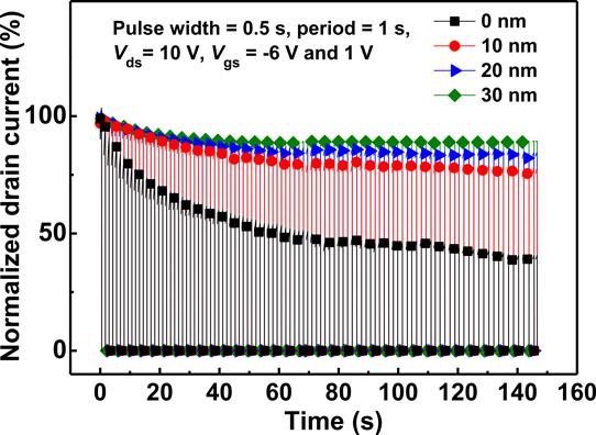
Figure 1: Transient on–off characteristics of MES-HEMTs and MOS-HEMTs with different SiO thicknesses.
The off-state breakdown (-10V gate potential, 1mA/mm leakage drain current compliance threshold) occurred at 236V with 30nm SiO, a 100V increase from 136V for the MES-HEMT. The breakdown strength (breakdown voltage divided by gate-drain spacing) was 39V/μm for 30nm SiO and 23V/μm for the MES-HEMT. The researchers comment: “The breakdown mechanism has been found to be caused by impact ionization, which can be triggered by gate leakage injection into the channel at high electric fields. The breakdown voltage is enhanced in our MOS-HEMTs due to the suppression of gate leakage by the SiO gate dielectric.”
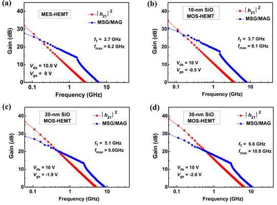
Figure 2: Small-signal characteristics of (a) MES-HEMTs and MOS-HEMTs with (b) 10nm, (c) 20nm, and (d) 30nm SiO. Drain bias 10V, gate potential set for maximum transconductance at 0V, -0.5V, -1.9V, and -2.6V, respectively.
Frequency-dependent measurements up to 20GHz gave current gain cut-off and maximum oscillation frequencies of 6.6GHz and 10.8GHz, respectively, for the MOS-HEMT with 30nm SiO (Figure 2). The comparable figures for the MES-HEMT were 2.7GHz and 6.2GHz. The improvement in the SiO device is suggested to be due to a lower gate capacitance, compared with the MES-HEMT. The (cut-off)x(gate-length) product was 13.2GHz-μm, higher than other values for scaled GaN HEMTs, according to the researchers. It is to be hoped that scaling the SiO MOS-HEMT structure will therefore lead to promising high-frequency performance.
Thermally evaporated SiO GaN MOS-HEMTs MOCVD
https://doi.org/10.1088/1361-6641/aad8d7
The author Mike Cooke is a freelance technology journalist who has worked in the semiconductor and advanced technology sectors since 1997.


