


- News
1 November 2018
Quantum cascade superluminescent arrays for mid-infrared applications
Researchers based in China have developed ~5μm-wavelength mid-infrared quantum cascade superluminescent emitters (QCSLE), in single and array formats [Jialin Sun et al, Optics Letters, vol43, p5150, 2018]. The team from Suzhou Institute of Nano-Tech and Nano-Bionics (SINANO), Institute of Semiconductors, and University of Science and Technology of China, sees potential for biomedical imaging, security inspection and gas detection from using QCSLEs as broadband light sources.
A particular application could be optical coherence tomography (OCT), which is widely used for human tissue imaging. In the near-infrared (NIR) such techniques have achieved high resolution in a non-invasive, non-contact manner. The team comments: “It is noteworthy that most biological tissues absorb much more photons within the mid-infrared (MIR) spectral range compared to the NIR range, indicating that a MIR-OCT could contain strong overtone and combination vibrational absorption bands of the spectral response to molecular species.”
The paper reports “for the first time, to the best of our knowledge”, a compact light emitter array with a very high room-temperature continuous-wave (RT-CW) light output power of 2.4mW. Such RT-CW operation is seen as a crucial requirement for MIR-OCT.
Superluminescent devices use amplified spontaneous emission to give high-power, low-coherence light. SLEs use a single-pass structure, so spontaneous photons are amplified, but lasing does not occur. To ensure single-pass behavior, it is necessary that the waveguide structure that transmits light out, rather than being trapped in multiple reflections as in lasers.
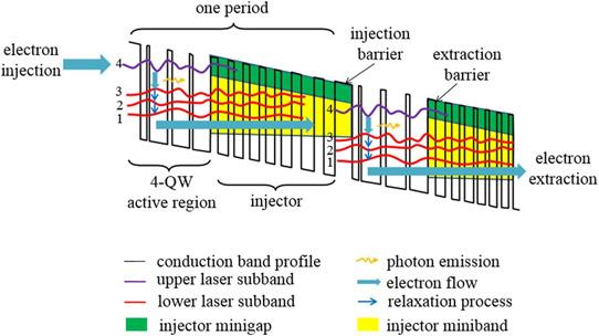
Figure 1: Band structure of four-QW coupling and two-phonon-resonance-based QC energy level.
The active layers of the QC structure were grown by solid-source molecular beam epitaxy (SS-MBE) on indium phosphide. The active region of the cascade section (Figure 1) was four coupled strain-compensated quantum wells (QWs) of indium gallium arsenide in indium aluminium arsenide (In0.678Ga0.322As/In0.365Al0.635As). The structure used a two-phonon resonance structure to improve depopulation of the lower state, enabling increased amplification. At the same time, the four wells enhanced spontaneous emission. The device material consisted of 30 repetitions of the cascade section design separated by low-doped n-InGaAs. The target emission wavelength was ~5μm.
The material was fabricated into double-trench narrow-ridge ‘W’-shaped waveguide structures 7μm deep. The ridge width was 10μm, and the trench widths were 20μm. Plasma-enhanced chemical vapor deposition (PECVD) silicon dioxide, 200nm thick, was used as insulation. Contact windows, 3μm wide, were etched in a reactive-ion process. The top contact metals were titanium/gold. The bottom contact consisted of germanium/gold/nickel/gold. The devices were mounted epitaxial-side down on copper heatsinks.
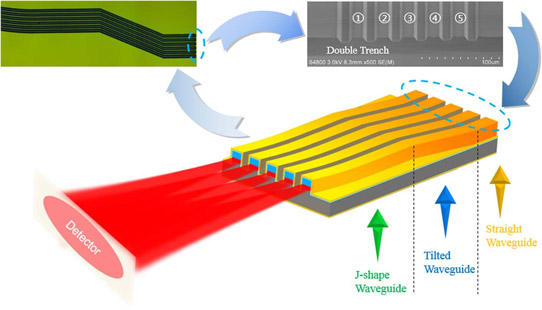
Figure 2: Bottom: schematic diagram of array device. Top-left: microscope image of 5-array. Top-right: corresponding scanning electron microscope image of rear end.
The waveguide was shaped with a 1mm-long tilted section connected to 0.5mm-long straight and 2mm-long ‘J’ sections (Figure 2, SLE 1). The researchers comment: “This design can create two mutations of refractive index in the waveguide to achieve a rather low reflectivity with a fairly small geometry, and hence provide an opportunity to fabricate array devices.”
Two further devices (SLE 2 and SLE 3) were produced giving a shorter ‘J’ section of 1.5mm. This reduced the angle between the tangent to the end of the ‘J’-section and the output facet normal from 9° to 4°. One of these latter devices also included a high-reflection coating on the rear facet (SLE 3).
The maximum output powers for three different structures were 1.6mW (at 1.75A, SLE 1), 2.2mW (at 1.85A, SLE 2) and 3mW (at 1.9A, SLE 3). The slope efficiency of SLE 3 was 0.0028W/A, about twice that of SLE 1.
Compact SLE arrays with up to 7 devices were based on the SLE 3 structure. The arrays were characterized in ‘quasi-continuous wave’ mode – 5μs pulses with 20kHz repetition (10% duty cycle) – at room temperature. The best performances were delivered by 3-SLE and 5-SLE arrays: 8.5mW output at 5.5A, and 12mW at 7A, respectively. The 7-array suffered from “excess thermal generation and low current density”. The turn-on voltage of the 7-array was ~12V, compared with ~9V for a single SLE 3 device.
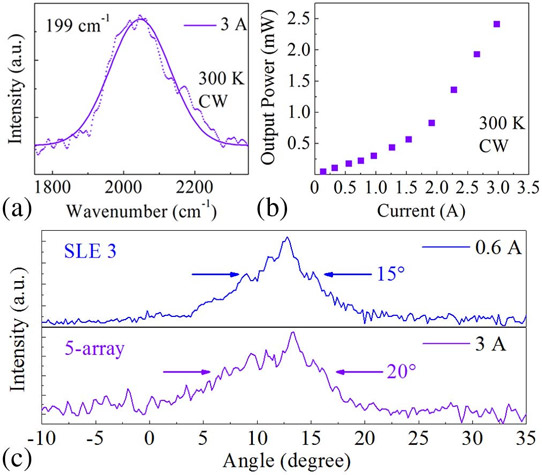
Figure 3: (a) Emission spectrum and (b) light–current curve measured from 5-array under CW mode at 300K. Lines correspond to Gaussian fitting to spectra. (c) Comparisons between far-field profiles of SLE 3 and 5-array.
Continuous-wave operation of the 5-array gave an output power of 2.4mW at 3A with 199/cm full-width at half maximum (FWHM) – see Figure 3. The researchers comment: “The high output power can increase the penetrating depth of light, the broad spectral width can enhance the axial resolution of the images, and the high-quality output beam can be effectively coupled into fiber, so the QC array device has been demonstrated as an ideal broadband light source for realizing the MIR-OCT system.”
Mid-infrared quantum cascade superluminescent emitters MBE InGaAs
https://doi.org/10.1364/OL.43.005150
The author Mike Cooke is a freelance technology journalist who has worked in the semiconductor and advanced technology sectors since 1997.


