


- News
30 November 2018
Gallium nitride vertical-channel junction field-effect transistors
RWTH Aachen University in Germany claims the first experimental realization of vertical-channel junction field-effect transistors (vc-JFETs) in a gallium nitride (GaN) epitaxial structure [Simon Kotzea et al, IEEE Transactions On Electron Devices, published online 26 October 2018]. One of the researchers involved is also associated with AIXTRON SE, a producer of metal-organic chemical vapor deposition (MOCVD) equipment.
Vertical devices are attractive for high-power-density applications since the structure pushes peak electric fields away from surfaces into the bulk material, avoiding the need for surface passivation or field plates.
The researchers used lower-cost 2-inch sapphire substrates to produce quasi-vertical vc-JFETs by MOCVD. The back-side ‘virtual’ contact was achieved using a heavily n-type doped GaN layer (Figure 1). A true vertical device would have the drain contact conducting through the back-side of the wafer – this is not possible using insulating sapphire.

Figure 1: Schematic of quasi-vertical vc-JFET with selectively regrown p-GaN gate areas.
Most research on vertical devices uses the much more expensive option of free-standing or bulk GaN, allowing true vertical structures. In production, where cost would be a critical consideration, there would be several possible routes to true vertical devices – removal of the substrate or the use of conducting growth substrates such as free-standing or bulk GaN or silicon. The penalty for using silicon is lower material quality that increases leakage currents.
The RWTH device structure was grown by first applying a 2μm lightly doped n-GaN drift layer and a 20nm heavily doped n-GaN contact layer, followed by selective-area regrowth of heavily doped p-GaN using silicon dioxide as the hard mask protecting the channel during etching and MOCVD. The gate-to-gate (GTG) distance was 4μm. The channel width was 54μm.
The etching for the selective-area regrowth used a combination of dry and wet steps. The sidewalls of the channel were aligned with the m-plane of the GaN crystal structure to reduce dry etch roughness. Wet tetramethylammonium hydroxide (TMAH) treatment further flattened the sidewalls and removed etch damage from the c-plane surface at the bottom of the etch. After the p-GaN regrowth, the material was activated by annealing at 900°C for 900 seconds in nitrogen. The aim of the annealing was to remove hydrogen from the magnesium doping. Hydrogen-magnesium complexes interfere with the desired generation of holes in p-GaN material.
Metallization of the device consisted of titanium/aluminium/nickel/gold for the drain and source, and nickel/gold for the p-GaN gate. The drain electrode was deposited first, followed by the gate, and finally the source. The drain and gate electrodes were annealed at 830°C and 535°C, respectively. The source electrode was not annealed due to the temperature restriction of the p-GaN contact.
The drain contact was ohmic with 0.8Ω-mm contact resistance. However, the gate contact was non-linear with 900Ω-mm contact resistance at zero bias, while the source demonstrated Schottky-like behavior. These problems were related to the non-annealed nature of the source contact and the absence of a heavily doped p-GaN layer under the gate electrode.
The gate electrode allows modulation of the thickness of the depletion layer at the pn junction, choking off current in the channel region between the source and drain. The drift layer was of ‘moderate’ thickness, reducing the expected breakdown performance. The aim of the moderate drift layer was to allow easier access to the virtual back contact through dry etching.
Given the Schottky-like ‘source’ contact, the researchers decided to reverse the drain bias so the devices were operated as if the source was the drain and vice versa. The behavior of the devices including the Schottky turn-on voltage of around 0.5V delayed the current increase with drain bias. The specific on-resistance was 2.36mΩ-cm2, normalized to the channel cross-section area. The gate leakage was two orders of magnitude lower than the drain current with gate potentials of magnitude up to 10V.
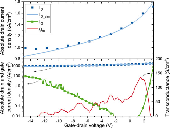
Figure 2: Drain and gate currents, and transconductance, transfer characteristics of quasi-vertical vc-JFET at 1V source-drain bias. Normalization to channel cross-section.
Although the transistor did not pinch-off, the gate potential did modulate the drain current (up to a factor of 1.8 with the gate at -10V, Figure 2). Pinch-off would occur at around -112V, according to simulations. Bringing this in the single-digit range would require scaling the dimensions down, along with reducing the channel doping to increase the range of the space-charge region. The simulations suggested that the space-charge region only extended 1μm in from both sides of the 4μm gate-to-gate gap at -12V.
The simulations also suggested that normally-off enhancement-mode operation would result from a 1μm gate-to-gate distance, along with 5μm channel length and 5x10¹⁵/cm3 doping, giving a +2.3V threshold. The drift/channel doping of the experimental device was 1x10¹⁶/cm3, according to mercury capacitance-voltage profiling measurements.
https://doi.org/10.1109/TED.2018.2875534
The author Mike Cooke is a freelance technology journalist who has worked in the semiconductor and advanced technology sectors since 1997.


