


- News
9 May 2018
Indium arsenide quantum dot laser on silicon from molecular beam epitaxy
Japan’s University of Tokyo claims the first electrically pumped 1.3μm indium arsenide (InAs) in gallium arsenide (GaAs) quantum dot (QD) lasers directly grown on on-axis (001) silicon (Si) substrates using molecular beam epitaxy (MBE) exclusively as the material growth process [Jinkwan Kwoen et al, Optics Express, vol26, p11568, 2018].
On-axis growth on (001) Si is usually initiated by metal-organic chemical deposition (MOCVD) before MBE QD layers. Alternative techniques that allow MBE seeding involve offcut substrates to avoid crystal defects such as threading dislocations (TDs), antiphase boundaries (APBs) and cracks. Unfortunately, off-axis Si is not compatible with mainstream CMOS-based electronics. MOCVD is not able to filter dislocations effectively or produce QDs with efficient luminescence.
The team sees the development of the 1.3μm laser as contributing to the push for silicon photonics “to solve the problems of metal wiring such as low bandwidth density and high-power consumption” for next-generation computing.
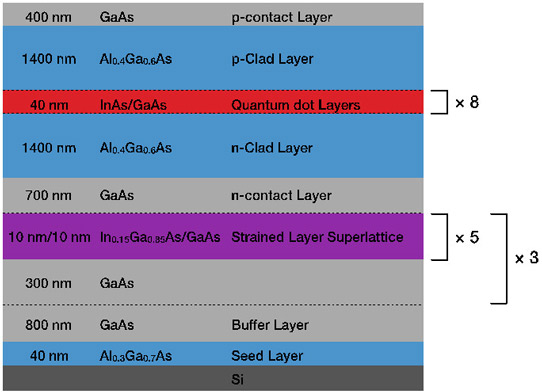
Figure 1: Schematic of InAs/GaAs QD laser material grown on on-axis Si (001) substrate.
The researchers used n-type substrates for the solid-source MBE (Figure 1). The chamber was first heated to 950°C for 5 minutes of substrate annealing. Threading dislocations were inhibited from reaching the QD layers by growing a series of three 300nm GaAs layers followed by InGaAs/GaAs strained superlattices. The threading dislocation density in the QD region was estimated at 5x10⁷/cm2. The team points to thermal cyclic annealing during deposition as a possible route to even lower density.
Anti-phase boundaries were avoided by a relatively high 500° growth temperature and high growth rate (1.1μm/hour) for the AlGaAs seed layer, enabling APB annihilation within 400nm of the GaAs buffer deposition.
The QDs measured about 30nm laterally with a density of 5x10¹⁰/cm2. The photoluminescence from the structure had 80% of the intensity from a structure grown on GaAs substrate. The peak wavelength was at 1250nm with 31meV full-width at half maximum. An excited level at 1150nm (+86meV) was also visible in the spectrum.
The material was fabricated into 80μm-wide broad-area Fabry-Perot lasers. The contacts were gold-germanium-nickel/gold. The back-side of the substrate was thinned to 100μm. The structures were then cleaved into 2mm-long lasers. The mirror facets were formed as-cleaved without applying high reflectivity coatings.
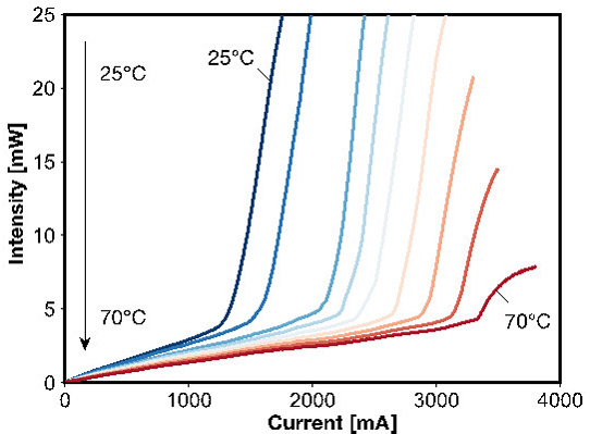
Figure 2: Temperature-dependent light output power versus current curves for laser under pulsed injection.
Under pulsed injection, the lowest lasing threshold current density was 320A/cm2. The maximum output power from a single facet was more than 30mW. The characteristic temperature for the laser threshold was 51K in measurements made in the range 25-70°C. At 25°C, the slope efficiency was 0.052W/A. The devices did not lase under continuous-wave current injection up to 1000mA.
The researchers admit that the laser grown on silicon demonstrated “degradation of several characteristics such as the output and thermal characteristics”, compared with devices on GaAs substrate. The lower quality of the GaAs buffer layer and the broad mesa width were blamed. The team hopes that optimization of the growth process, particularly of the seed layer, will improve laser performance. Narrower mesas should also improve current constriction and thermal management.
InAs GaAs QD lasers Si substrates MBE
https://doi.org/10.1364/OE.26.011568
The author Mike Cooke is a freelance technology journalist who has worked in the semiconductor and advanced technology sectors since 1997.


