


- News
2 May 2018
Near-ultraviolet optoelectronic transmitter/receiver system
Researchers in China and Japan have used III-nitride on silicon (Si) technology to create integrated near-ultraviolet (NUV) optoelectronic transmitter/receiver systems [Chuan Qin et al, Appl. Phys. Express, vol11, p051201, 2018]. The monolithic devices were released from the silicon growth substrate and transferred to glass on a test pad. The NUV light was emitted and detected by indium gallium nitride (InGaN) multiple quantum wells (MQWs) in aluminium gallium nitride (AlGaN) barriers. The light transfer was enabled by an integrated waveguide.
The team from Nanjing University of Posts and Telecommunications and Zhengzhou University in China and Nagoya University in Japan suggests that the platform could be used for on-chip power monitoring of light-emitting systems, free-space light communication, and wearable optoelectronics in the NUV region. The advantages of using silicon substrates include low material cost and potential for mass production from larger-diameter wafers.
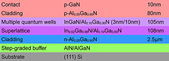
Figure 1: Epitaxial structure.
The researchers grew III-N films on (111) Si (Figure 1). This material was used to fabricate the multi-component optoelectronic system (Figure 2). Inductively coupled plasma reactive ion etching created two isolation mesas for the transmitter and receiver sections, and exposed the n-AlGaN contact layer. The p- and n-contact electrodes consisted of nickel/silver, which can also function as mirrors directing light out of the bottom of the structure. Further etching created the 6μm-wide, 100μm-long optical waveguide connection between the devices, and the support beams for the membrane formation.
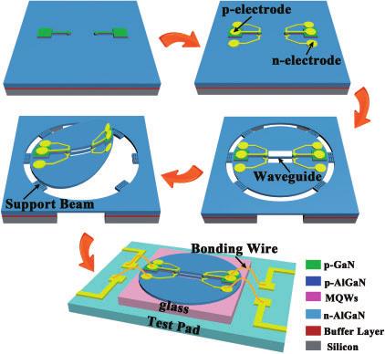
Figure 2: Schematic of fabrication, release, transfer and wire-bonding process flow for monolithic NUV multi-component system.
The release of the silicon substrate was prepared by applying a photoresist to the wafer top side as protection. Deep reactive ion etching removed the silicon to give suspended membranes. The III-nitride layer was then thinned with further etching from the back side. The 0.8mm-diameter device structure was released and transferred to a foreign substrate. The system was then connected to the test pad by wire bonding.
The turn-on voltages of the MQW diodes were 2.8V. The peak wavelengths of the devices shifted after the transfer due to changes in internal stresses that affect the electric fields in the devices due to the charge polarization of the various III-nitride atomic bonds. The dominant electroluminescence peak was at 386nm after transfer to glass. The response function peak of the MQW diode (operated as a photodiode receiver) is blue-shifted toward ~372nm, but there was some overlap for detection.
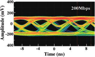
Figure 3: Eye diagrams for free-space light communication at transmission rate of 200Mbps.
Non-return-to-zero on–off keying modulation, with 3.5V peak-to-peak signals and 2.2V offset, produced open eye diagrams at 200 megabits per second (Mbps) pseudorandom binary sequence (PRBS) data streams (Figure 3).
Near-ultraviolet optoelectronic transmitter/receiver InGaN AlGaN
https://doi.org/10.7567/APEX.11.051201
The author Mike Cooke is a freelance technology journalist who has worked in the semiconductor and advanced technology sectors since 1997.


