


- News
30 May 2018
Room-temperature photoluminescence from III-IV-V semiconductor alloys
Massachusetts Institute of Technology in the USA claims significant room-temperature photoluminescence (PL) “for the first time in high-quality III-IV-V alloys grown by metalorganic chemical vapor deposition” [Roger Jia et al, J. Appl. Phys., vol123, p175101, 2018]. A modified growth process was used to inhibit phase separation, which can quench PL. Instead, the alloys did exhibit some small-scale composition fluctuation, as seen in many III-V alloys.
The effect of the composition fluctuation was to give a narrower effective bandgap than expected from simple extrapolations between the gap of gallium arsenide (GaAs) and that of the germanium (Ge) or silicon germanium (SiGe) group IV component. In the case of (GaAs)1-x(Ge2)x, the narrowing limited the bandgap to less than 0.8eV. Adding silicon enabled wider bandgaps to be accessed.
The team writes: “We have apparently created what is effectively a Ge-like solid penetrating a GaAs lattice, resulting in optical properties similar to those of Ge but with a direct-bandgap nature.”
The researchers expect III-IV-V alloys to exhibit “interesting electrical, optical and thermoelectric properties on previously unattainable lattice constants.”
In terms of potential applications, the team sees potential for a 1eV bandgap, filling a void in multi-junction photovoltaic designs, along with narrower bandgaps for efficient infrared detection using direct-bandgap material. The usual suspects for such bandgaps suffer from lattice mismatches or the need to be grown on very expensive small-diameter substrates.
The epitaxial materials were grown on semi-insulating (001) GaAs substrate. The precursors were trimethyl-Ga (Ga(CH3)3), along with arsine (AsH3), silane (SH4), and germane (GeH4). The alloy films were deposited after 40nm GaAs homoepitaxy and 20-second anneal in nitrogen (N2). Various temperatures between 575°C and 700°C were used for the alloy growth, while the pressure was a constant 250Torr.
The team explains: “Our decision to conduct a 20s N2 ambient anneal prior to depositing the alloy stems from previous studies, indicating that As-rich surfaces are unfavorable for Ge adatom incorporation. Since the alloys are formed by co-deposition of Ga, Ge and As, an As-rich substrate surface may cause increased segregation of Ge toward the surface as Ga and As incorporate into the film.”
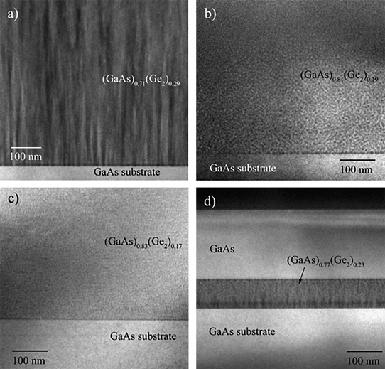
Figure 1: (002) Dark-field XTEM images of (GaAs)1-x(Ge2)x alloys. Growth temperature: (a) 700°C, (b) 650°C, (c) 575°C, (d) 650°C. Last image also includes 200nm GaAs overlayer. Relatively darker regions contain more Ge compared to lighter regions.
Diffraction studies using cross-sectional transmission electron microscopy (XTEM) found single crystal material, but with non-uniform composition. The morphology of the non-uniformity was striated or speckled, according to nominal composition (Figure 1). The difference is believed to be due to varying surface mobility of adatoms, due to the different growth temperatures. Speckled structures arise where the adatoms are less mobile at lower temperatures, giving short-lived variations in composition. Higher mobility allows adatoms to move and feed composition variations in the vertical direction of growth.
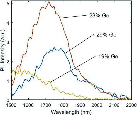
Figure 2
Room-temperature photoluminescence (PL) studies revealed peaks at 1550nm (0.8eV), 1720nm (0.72eV) and 1760nm (0.7eV), for samples with 19%, 23% and 29% Ge2, respectively (Figure 2). Samples with large phase separation did not show PL peaks. At 77K, the 29% striated sample showed several peaks, while the speckled 19% material maintained a single peak. The multiple peaks of the 29% material was attributed to different compositions in the striations.
In addition, a sample with 100nm (GaAs)0.77(Ge2)0.23 alloy layer that was subjected to further growth of 200nm GaAs was found to be free of anti-phase boundaries (APBs). Such APBs are normally found with GaAs deposition on exact (001) germanium.
The MIT team also grew (GaAs)0.8(Si0.1Ge0.9)0.2 and (GaAs)0.84(Si0.1Ge0.9)0.16, using 650°C and 575°C temperatures, respectively. Photoluminescence on these samples gave blue-shifted PL spectra, reflecting the wider bandgap of silicon, compared with germanium. The team comments: “This result suggests the possibility of engineering the range of low bandgaps above 0.8eV using III-IV-V alloys as an alternative to finding the growth conditions needed to fully inhibit composition fluctuations in (GaAs)1-x(Ge2)x , which thus far remains elusive.”
The researchers also hope that narrower bandgaps could be accessed by using phosphide or antimonide alloys.
https://doi.org/10.1063/1.5016443
The author Mike Cooke is a freelance technology journalist who has worked in the semiconductor and advanced technology sectors since 1997.


