


- News
25 May 2018
Strain engineering higher hole density in N-polar aluminium gallium nitride
Jilin University in China and King Abdullah University of Science and Technology (KAUST) in Saudi Arabia have used strain engineering in graded nitrogen-polar (N-polar) p-type aluminium gallium nitride (p-AlGaN) layers to boost hole density [Long Yan et al, Appl. Phys. Lett., vol112, p182104, 2018]. The metal-organic chemical vapor deposition (MOCVD) technology enabled a significant increase in luminescence from indium gallium nitride (InGaN) multiple quantum well (MQW) light-emitting diodes.
Low hole density in p-AlGaN layers normally arises because of an activation energy that increases with aluminium concentration. By grading AlGaN composition, the researchers set up strain fields that altered the charge polarization and created fixed charges that alter the activation level of magnesium acceptor doping through field ionization. The technique has previously been developed on metal-polar and N-polar p-AlGaN grown by molecular beam epitaxy (MBE). For MOCVD, the technique has been used successfully for metal-polar structures, but N-polar layers suffer from high background electron concentrations that hinders the method’s effectiveness.
The materials were grown using MOCVD on sapphire. First, a 2μm N-polar GaN template layer was deposited, followed by 75nm 1020°C magnesium-doped p-AlGaN with composition graded from 0% to 30% Al. The grading was achieved by varying the flow rates of trimethyl-Al and trimethyl-Ga precursors. The magnesium acceptors were activated with 720°C annealing in nitrogen. The AlGaN layer properties were compared with those of another sample with 100nm magnesium-doped GaN on 2μm GaN template layer.
X-ray studies suggested the AlGaN grading was linear. Also, the x-ray measurements implied that there was no tensile strain relaxation in the AlGaN. It follows from this that the charge polarization arising from the strain should be in the same direction as that arising spontaneously from the AlGaN crystal structure. The researchers comment: “In the fully strained graded AlGaN layer, the magnitude of piezoelectric polarization increases with the increasing Al content, which is the same as the trend of spontaneous polarization. Therefore, the fully strained state in the graded AlGaN layer can further increase the polarization gradient.”
The change (divergence) in the polarization gives rise to a polarization charge density, estimated at 2x10¹⁸/cm3 for the p-AlGaN layer. Theoretically, the field-ionized holes from the magnesium acceptors should balance this fixed charge density.
Hall measurements actually gave a hole density in the p-AlGaN layer of 6.4x10¹⁷/cm3. This compares with 3.7x10¹⁶/cm3 for the p-GaN comparison sample, down a factor of 17. Furthermore, the hole density in the p-AlGaN was much less temperature-dependent over the range 150-450K (Figure 1).
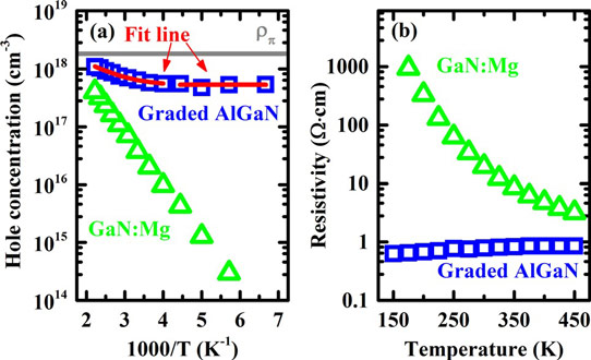
Figure 1: Temperature-dependent hole concentration (a) and resistivity (b) of graded p-AlGaN and p-GaN layers. Gray line indicates concentration of polarization-induced volume charges predicted by theory. Red line is the fit for model including effects of thermally activated and field-ionized holes.
The team comments: “The absence of freeze-out in the graded AlGaN layer reveals that the holes in the graded AlGaN layer are mainly created by the polarization electric field. Besides, it is worth noting that the measured hole concentration of the graded AlGaN layer is lower than the density of polarization charge (the gray solid line).”
The difference between the 6.4x10¹⁷/cm3 hole density and the 2x10¹⁸/cm3 polarization charge density of the p-AlGaN is speculatively attributed to “the screening effect caused by defects”.
The increased hole density in the p-AlGaN was also reflected in the 300K resistivity of the layer – 0.8Ω-cm, compared with 19.6Ω-cm for the p-GaN comparison.
Inserting a silicon nitride mask into the GaN template layer increased the p-AlGaN hole density to 7.9x10¹⁷/cm3. It has been found that silicon nitride decreases the density of oxygen donors that reduce hole density by compensation effects. Further increase in the hole density to 9.0x10¹⁷/cm3 came with optimizing the magnesium acceptor doping.
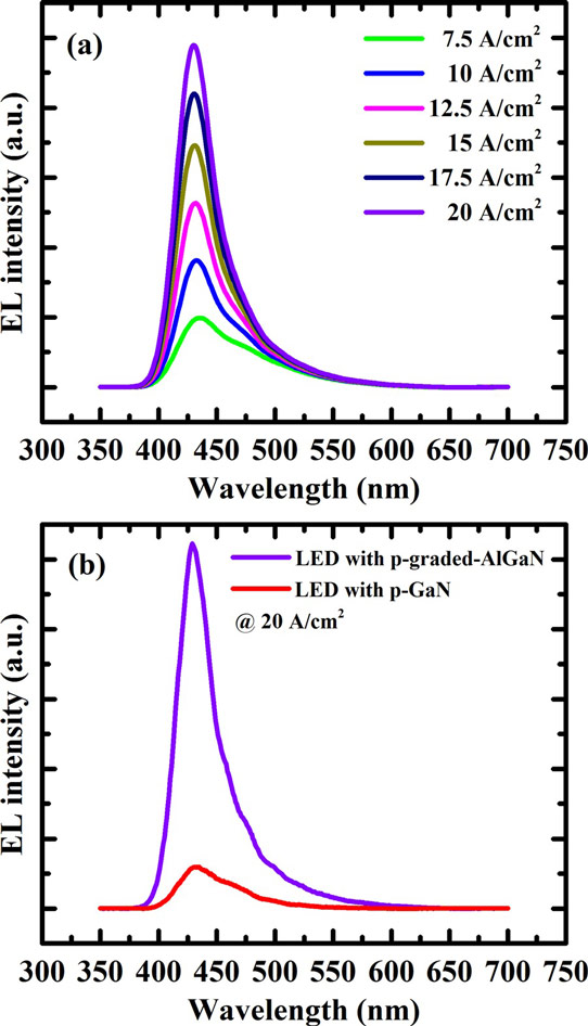
Figure 2: (a) LED spectra with graded p-AlGaN at various injection current densities. (b) LED spectra with p-GaN and graded p-AlGaN hole injectors at 20A/cm2 current density.
The researchers finally used the technology to create InGaN MQW LEDs. The MQW consisted of five wells. The p-type contact layer used the optimized p-AlGaN or, for comparison, p-GaN. The p-AlGaN device had peak wavelengths of 435nm and 420nm at 7.5A/cm2 and 20A/cm2 injection, respectively (Figure 2). The wavelength shift was attributed to free-carrier screening of the charge polarization fields in the MQW region. The p-AlGaN LED had much higher intensity than the p-GaN comparison device, thanks to the higher hole concentration.
https://doi.org/10.1063/1.5023521
The author Mike Cooke is a freelance technology journalist who has worked in the semiconductor and advanced technology sectors since 1997.


