


- News
19 March 2018
Semi-polar III-nitride integration for visible light communication
Researchers based in Saudi Arabia and USA have used semi-polar indium gallium nitride (InGaN) quantum wells (QWs) to create a laser diode (LD) integrated with a semiconductor optical amplifier (SOA) for visible light communication (VLC), smart lighting, and underwater wireless optical communications (UWOC) [Chao Shen et al, Optics Express, vol26, pA219, 2018].
The team from Saudi Arabia’s King Abdullah University of Science and Technology (KAUST), University of California Santa Barbara (UCSB) in the USA, and King Abdulaziz City for Science and Technology (KACST) in Saudi Arabia, comments: “Since the on-chip integration of various photonic devices offers the advantages of small footprint, low cost and multi-functionality, it is of great interest to develop III-nitride photonic integrated circuits (PICs) at the visible wavelength.”
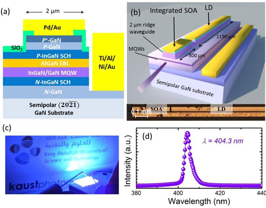
Figure 1: (a) Cross-sectional layered structure and (b) three-dimensional illustration of 405nm-emitting dual-section integrated SOA-LD on semi-polar GaN substrate. Inset: fabricated device under optical microscope. (c) Photo of device operating at room temperature. (d) Emission spectrum of device at laser gain section current of 250mA and zero SOA section driving voltage, showing peak at ~404.3nm.
The epitaxial structure for the device was grown by metal-organic chemical vapor epitaxy on semi-polar (20-2-1) GaN. The active light-emitting region was four pairs of In0.1Ga{0.9N/GaN quantum wells/barriers. A 16nm Al0.18Ga0.82N layer served as an electron-blocking layer (EBL). The separate-confinement heterostructure (SCH) waveguides consisted of 60nm/60nm p-/n-In0.025Ga0.975N. The p- and n-GaN cladding layers were 600nm and 350nm, respectively.
The p- and n-electrodes were palladium/gold (Pd/Au) and titanium/aluminium/nickel/gold (Ti/Al/Ni/Au), respectively. The structure of the separate SOA and laser diode sections were defined by patterned etching of a 2μm-wide ridge. Electrical separation of the devices was achieved by etching the p-GaN contact layer between them, while maintaining a seamless optical connection.
When the SOA was unbiased, the light output power was low due to optical losses. The light output increased as the SOA bias increased to 6.25V. In fact, beyond 5V bias, the output was greater than for a laser diode without SOA, suggesting light amplification in the SOA itself beyond 4V bias.
With a laser diode current of 250mA, the light output power increased from 8.2mW to 30.5mW as the SOA bias increased from 0V to 6.25V. Between the same SOA biases, the laser threshold current decreased from 229mA to 135mA. With the laser diode at 250mA, the SOA current at 6V bias was 67mA, giving a total input power of 2.14W and wall-plug efficiency (WPE) of 1.3%. A separate laser diode with 317mA (250mA+67mA) current injection had a WPE of 0.54%.
The rate of increase in effective gain of the SOA as the bias increased from 4V to 6.25V was 2.36dB/V at 250mA laser diode injection. The team comments: “The high gain observed in the device is partially attributed to the large electron-hole wavefunction overlap in InGaN/GaN QWs grown on semi-polar (20-2-1) GaN substrate, which exhibits reduced polarization field compared to that in conventional [polar] c-plane devices.” The peak amplification ratio between 0V and 6.25V SOA bias was 18.4 at 404nm wavelength and 200mA laser diode injection.
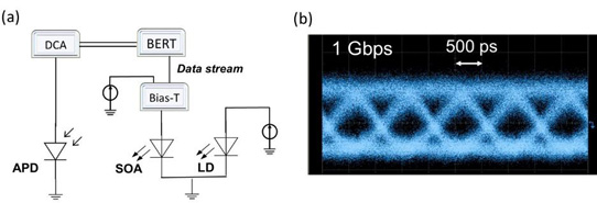
Figure 2: (a) Schematic of non-return-to-zero on-off keying modulation (NRZ-OOK) data transmission measurement using SOA-LD as transmitter and avalanche photodiode (APD) as receiver, along with bit error rate tester (BERT) and digital communication analyzer (DCA). (b) Eye diagram of 1Gbit/s data rate.
The combined device achieved ‘open eye’ data transmission at 1 gigabits per second (Gb/s) with SOA modulation and constant 250mA laser diode injection (Figure 2). The bit error rate was 3.4x10⁻⁴, meeting the limit for forward error correction (FEC) of 3.8x10⁻³.
Semi-polar InGaN AlGaN Laser diode SOA
https://doi.org/10.1364/OE.26.00A219
The author Mike Cooke is a freelance technology journalist who has worked in the semiconductor and advanced technology sectors since 1997.


