


- News
28 March 2018
Tunneling to green light emission with improved efficiency performance
Researchers based in USA and Saudi Arabia have used tunnel junctions (TJs) to improve the efficiency performance of indium gallium nitride (InGaN) green light-emitting diodes [Abdullah I. Alhassan et al, Appl. Phys. Express, vol11, p042101, 2018]. The team from University of California Santa Barbara (UCSB) and King Abdulaziz City for Science and Technology (KACST) used a combination of metal-organic chemical vapor deposition (MOCVD) and molecular beam epitaxy (MBE) to allow high-quality n-type material to be grown on top of p-GaN and the thermally unstable InGaN quantum wells (QWs).
The TJ layers are seen as being an alternative to transparent conductive oxides (TCOs) for current spreading, allowing for more uniform current conduction and reducing peak current density. High current density reduces the efficiency of conversion of electrons and holes into photons. GaN TJs also absorb less green light compared with the most popular transparent conductor, indium tin oxide (ITO).
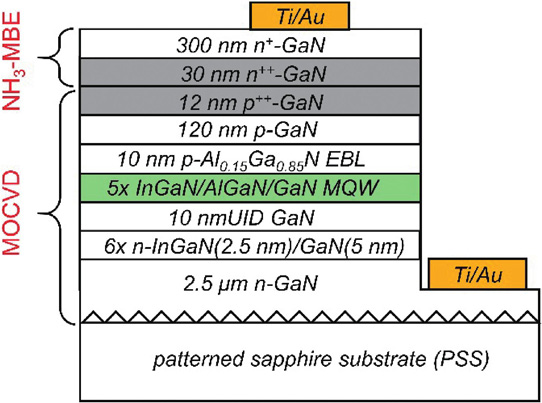
Figure 1: Cross-sectional schematic of LED structure processed with TJ contact.
The LED structure (Figure 1) was grown by atmospheric-pressure MOCVD up to the p-GaN layer. The substrate was patterned sapphire with a 1μm unintentionally doped (UID) GaN template layer.
The undoped active region consisted of five periods of 2.7nm InGaN quantum wells, a 2nm aluminium gallium nitride (Al0.3Ga0.7N) cap, and a 9nm GaN barrier. Various indium contents were used to create material for LEDs emitting in the range 490-526nm.
The structure included an electron-blocking layer (EBL). The samples were annealed to activate the magnesium doping of the p-type layers. Excess magnesium was cleaned from the surface of the materials before MBE of the TJ layers. Before the MBE process, the materials were activated again by annealing at 600°C for 10 minutes in vacuum in the reaction chamber. The growth of the n-type GaN tunnel layers was carried out at 700°C.
Mesa-type LEDs were fabricated with titanium/gold (Ti/Au) contacts. Comparison devices were produced with the TJ replaced by ITO transparent conductor from electron-beam deposition. The ITO electrode was chromium/nickel/gold (Cr/Ni/Au). The TJ simplified the fabrication by not needing the Cr/Ni/Au deposition.
The devices were packaged in a vertical stand geometry so that light could be extracted from the top and bottom surfaces of the LED.
At 20A/cm2 current injection density, a green-emitting tunnel-junction device achieved an output power of 17mW, which compares with 15.6mW for the ITO LED. However, the TJ increased the forward voltage by 0.9V, increasing the power consumption. The researchers suggest that the penalty is due to a relatively low silicon concentration in the n++-GaN part of the TJ. A high silicon doping concentration should reduce the width of the depletion layer at the interface with the p++-GaN, which should increase the tunnel current.
The peak emission wavelength of the TJ-LED was 527nm at 20A/cm2 (20mA) injection. The peak wavelength shortened by about 10nm between 5mA and 40mA injection. The blue-shift was attributed to charge polarization-related effects in the MQW. Over the same current range, the full-width at half maximum increased from 32nm to 38nm. The ITO-LED showed similar spectral behavior. The FWHM at 20A/cm2 was 34nm.
While the two devices had similar peak ~41% external quantum efficiency (EQE) at 3A/cm2, at a current injection of 35A/cm2 the EQE of the TJ-LED was 31.2%, compared with 27% for the ITO device. The researchers comment: “The lower droop of the TJ LEDs may be attributed to the improved current-spreading uniformity in n-GaN compared with that of ITO, resulting in less current crowding. This reduction in current crowding leads to a reduction in local carrier density that mitigates efficiency droop.”
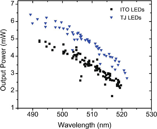
Figure 2: Dependence of electroluminescent output power on emission peak wavelength for ITO and TJ green LEDs at 35mA (35A/cm2). Output power was measured from the back side of wafers.
The researchers also studied the output powers of a series of devices emitting different wavelengths (490-526nm, Figure 2). The TJ-LEDs exhibited a higher power for a given wavelength. The power reduced as the wavelength extended further into the green region.
MOCVD MBE LEDs InGaN Gallium nitride tunnel-junction contacts
https://doi.org/10.7567/APEX.11.042101
The author Mike Cooke is a freelance technology journalist who has worked in the semiconductor and advanced technology sectors since 1997.


