


- News
21 March 2018
Silicon hole injector for deep ultraviolet aluminium gallium nitride diodes
Researchers based in the USA have used p-type silicon (p-Si) nanomembranes as hole injector layers for deep ultraviolet (DUV) light-emitting diodes (LEDs) emitting at 229nm [Dong Liu et al, Appl. Phys. Lett., vol112, p081101, 2018].
The team from University of Wisconsin-Madison, HexaTech Inc, University of Texas at Arlington, and Michigan State University, hope to overcome the low hole injection efficiency of p-type III-nitride materials such as aluminium gallium nitride (AlGaN) alloys, particular those with high aluminium fractions. Apart from boosting the efficiency of LEDs, the researchers also believe that p-Si nanomembrane hole injection layers may lead to DUV laser diodes in the future.
DUV devices are desired for applications such as biological and chemical detection, decontamination, medical treatment, high-density optical recording, and lithography. AlGaN alloys allow access to bandgaps of 3.3eV-6.2eV (GaN-AlN), giving wavelengths from 376nm down to 200nm. However, high-Al-content AlGaN devices with emission wavelengths shorter than 300nm have sharply decreasing efficiency. Poor hole injection and high defect densities are leading causes of inefficiency.
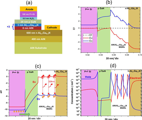
Figure 1: (a) Schematic of LED device. (b) Band diagram simulations at equilibrium and under 10V forward bias giving 300A/cm2 current density (c). (d) Calculated barrier concentration distribution across structure under forward bias.
Bulk AlN with low dislocation density of 104/cm3 was used as a substrate for low-pressure organometallic vapor phase epitaxy of the DUV structure (Figure 1). The 20nm p-GaN cap protects against rapid oxidation of the underlying Al-containing material.
The p-GaN was covered with 0.5nm aluminium oxide (Al2O3) from five cycles of atomic layer deposition (ALD). The 100nm p-Si nanomembrane hole injector had a heavy doping concentration of 5x10¹⁹/cm2. The Al2O3 acted and passivation and quantum tunnel barrier for hole injection.
The nanomembrane was released from a silicon-on-insulator (SOI) substrate and transferred to the III-nitride structure. Rapid thermal annealing at 500°C for five minutes was used to increase the strength of the Al2O3-p-Si bonding. Also, a very smooth epitaxial surface with root-mean-square roughness of 0.547nm aided the bonding process with the transferred p-Si, which resulted in 0.677nm roughness of the total structure.
The LED fabrication consisted of mesa isolation, exposure of the n-AlGaN contact for deposition of the titanium/aluminium/nickel/gold cathode, and deposition of the titanium/gold anode. The cathode and anode geometries were interdigitated to minimize losses from lateral current spreading resistance. The effective device area was estimated at 1.31x10⁻³cm2.
The LED turn-on voltage was about 7V. The reverse leakage was relatively high due to wafer growth dislocation defects, it is thought. The devices were operated in continuous wave (CW) mode without thermal management or cooling. No special light extraction enhancements were applied.
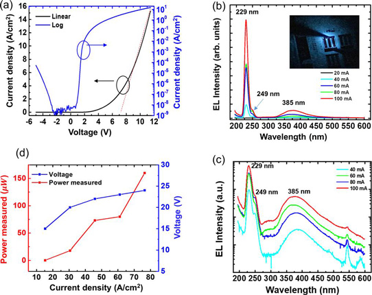
Figure 2: (a) Current density-voltage characteristics of typical LED on linear and log scales. (b) Electroluminescence (EL) spectra under different driving current densities with CW operation. Inset: optical microscopic image of forward-bias LED diode showing visible blue illumination. (c) Log-scale plot of EL spectra under currents of 40mA, 60mA, 80mA and 100mA. (d) Plot of measured light output power as a function of driving current density and associated voltages.
The peak wavelength was around 229nm. Parasitic peaks were also seen at 249nm DUV and ~380nm blue. These parasites were more than one order of magnitude less intense than the main peak. The 249nm peak is attributed to the 4.98eV bandgap of the n-AlGaN electron-injection layer. The researchers add: “The broad peak at 385nm in the visible range has multiple contributions, likely from the top p-GaN combined and with deep-levels in AlGaN, excited by 229nm photons.”
The output power reached 160μW at 24V bias and 100mA injection (76A/cm2). “The light emission at 229nm showed no significant efficiency droop up to 76A/cm2 in CW operation and without thermal management,” the researchers claim. The external quantum efficiency was 0.03%. The team believes this could be improved by thinning the AlN substrate to reduce point-defect absorption in the 229nm wavelength range.
https://doi.org/10.1063/1.5011180
The author Mike Cooke is a freelance technology journalist who has worked in the semiconductor and advanced technology sectors since 1997.


