


- News
13 June 2018
Gallium nitride tunnel junctions from pure MOCVD process for VCSELs
University of California Santa Barbara (UCSB) in the USA claims the first demonstration of a III-nitride semiconductor vertical-cavity surface-emitting laser (VCSEL) with a tunnel junction (TJ) on the p-side using only metal-organic chemical vapor deposition (MOCVD) material growth [SeungGeun Lee et al, Appl. Phys. Express, vol11, p062703, 2018].
Tunnel junctions are seen as an alternative to indium tin oxide (ITO) as a current-spreading material on the p-side of light-emitting III-nitride devices. Indium tin oxide increases laser threshold currents and absorbs light, reducing efficiency.
VCSELs offer desirable characteristics such as compactness, low thresholds, large modulation bandwidth, narrow linewidths, and circular beam patterns.
Tunnel junctions of heavily doped p- and n-type material have been created before for VCSELs, but the UCSB team reports that these have used hybrid growth processes involving MOCVD and molecular beam epitaxy (MBE). An MOCVD-only process is preferred since MBE is performed at lower temperatures, leading to higher defect density and impurity incorporation. Defects and impurities increase non-radiative recombination, reducing efficiency.
The VCSEL epitaxial material consisted of layers grown by MOCVD on bulk m-plane gallium nitride (GaN), miscut by -1° in the c-direction. Growth was carried out in two steps to allow activation of the buried p-type layers. Such layers suffer from hydrogen passivation, which hampers the acceptors from grabbing electrons to create holes in the valence band. An important aspect of activation is to drive out the hydrogen, usually with thermal annealing. Buried layers have less surface area – just the sidewalls – through which hydrogen can escape.
Between the initial growth and re-growth, the p++-GaN was treated with buffered hydrofluoric acid (BHF) to remove excess magnesium, reducing diffusion into the subsequent n++-GaN layer. When the wafer was returned to the MOCVD chamber, the temperature was held at 750°C for 5 minutes to activate in-situ the p-GaN material before MOCVD re-growth at 900°C.
The tunnel-junction structure was optimized with several experimental processes. A test structure with in-situ activation annealing had a 1.1V reduced forward voltage for a 1kA/cm2 current density. The performance of the in-situ activation was similar to a structure grown using a standard ex-situ anneal at 600°C for 10 minutes in air (less than 0.1V difference over the test range).
The effect of the buffered hydrofluoric acid treatment was a 0.5V reduction of forward voltage at 1kA/cm2. “We believe that the BHF treatment improved the voltage by reducing Mg diffusion into the n++-GaN layer, which could compensate electron carriers required to form an abrupt junction,” the researchers comment.
Combining the BHF treatment with in-situ activation gave tunnel junctions with 3.4V forward voltage at 20A/cm2 and 4.5V at 1kA/cm2, close to the performance of junctions grown using a hybrid MOCVD/MBE process (3.05V at 20A/cm2) by a similar research team based at UCSB.
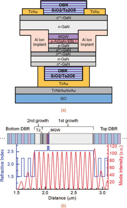
Figure 1: (a) Schematic of flip-chip VCSEL structure with dual dielectric DBRs and MOCVD-grown TJ contact and (b) cavity-mode intensity distribution overlaid with refractive index profile.
For the VCSEL (Figure 1, Table 1), the epitaxial structure was first grown to the p++-GaN layer, followed by mesa etch and aluminium (Al) ion implantation to form the device aperture. Then the tunnel junction growth was prepared with aqua regia and BHF treatments. After the tunnel-junction growth, a 17-period distributed Bragg reflector (DBR) consisting of silicon dioxide (SiO2) and tantalum pentoxide (Ta2O5) layers was deposited, followed by titanium/gold (Ti/Au) contact metals.
Table 1: VCSEL epitaxial layer structure grown on m-plane GaN substrate. (UID: unintentionally doped.)
| Epitaxial layer | Thickness | Doping concentration | Contribution to internal optical loss |
| 2nd growth | |||
| n+-GaN | 10nm | 1019/cm3 | 1.8% |
| n-GaN | 94nm | 1.3x10¹⁸/cm3 | 6.0% |
| n++-GaN | 40nm | 1020/cm3 | 9.4% |
| 1st growth | |||
| p++-GaN | 14nm | 2.2x10²⁰/cm3 | 21.7% |
| p-GaN | 61.2nm | 1019/cm3 | 12.8% |
| p-AlGaN | 5nm | 2.2x10¹⁹/cm3 | 1.3% |
| 2x(InGaN/GaN) MQW | 2x(1nm/14nm) | UID | |
| n-GaN | 759.4nm | 2.3x10¹⁸/cm3 | 45.7% |
| n+-GaN | 15nm | 1.7x10¹⁹/cm3 | 1.3% |
| InGaN (sacrificial QW) | 7nm | UID | |
| n-GaN (template) | ~1300nm | 1.3x10¹⁸/cm3 |
The device structure was then flipped and bonded onto metal layers consisting of titanium/nickel/gold/indium/gold (Ti/Ni/Au/In/Au) on a silicon carbide (SiC) substrate. The GaN growth substrate was removed by photo-electro-chemical etching of a sacrificial MQW. The VCSEL was completed with the deposition of Ti/Au contact metals and a 13-period DBR. The n++-GaN and DBR were separated by a 1/8-wavelength layer of Ta2O5.
The VCSEL was characterized using pulsed operation, presumably to avoid self-heating effects. The threshold for lasing occurred at 10kA/cm2 current density (15mA current) and 7.8V forward bias. The maximum output power was 319μW with 55kA/cm2 injection and 12V bias. Kinks in the output power behavior were likely due to higher orders contributing to the lasing. The wavelength was 408nm with ~1.9nm full-width at half maximum (FWHM) at 20mA injection. The accuracy of the linewidth was limited by the spectrometer’s resolution capability. The differential efficiency reached 0.28%
The differential resistivity of the tunnel junction was 10-4Ω-cm2, higher than the 5x10⁻⁵Ω-cm2 for the previously reported tunnel junction from a hybrid growth process. “We believe that the low doping concentrations of the current-spreading layers on the p-side are the main cause of the high differential resistivity that limits the device performance,” the researchers comment.
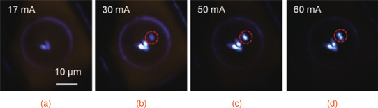
Figure 2: Optical microscopy images of VCSEL as function of current above threshold (∼15mA). Exposure times of camera were same for (a) and (b) and reduced for (c) and (d) to obtain clear images. Lasing spots in red circles show switching to higher-order mode.
Optical microscope inspection of the 14μm-diameter aperture during lasing showed lasing spots that increased in number as the injection current increased (Figure 2). Some of the lasing filaments were at the original frequency, others contributed higher modes. The non-uniformity is attributed by the team to poor current spreading and variations of the tunnel-junction contact resistance. The researchers also suggest that surface residues such as gallium oxide left after the GaN substrate removal could play a role in the non-uniformity.
GaN GaN tunnel junctions MOCVD VCSELs
https://doi.org/10.7567/APEX.11.062703
The author Mike Cooke is a freelance technology journalist who has worked in the semiconductor and advanced technology sectors since 1997.


