


- News
21 June 2018
High-material-yield halogen-free vapor phase epitaxy of gallium nitride
Toyota Central R&D Labs Inc in Japan has been exploring ways to improve gallium use in growing gallium nitride (GaN) by vapor-phase epitaxy (VPE) on sapphire [Daisuke Nakamura and Taishi Kimura, Appl. Phys. Express, vol11, p065502, 2018]. Fast growth by hydride VPE typically incorporates less than 10% of the source gallium metal. The Toyota researchers comment: “This low yield is probably due to several factors, including a reverse reaction (etching) and the presence of a thick stagnant boundary layer on the seed surface (since the process is carried out under atmospheric pressure).”
The US Geological Survey estimates the global annual supply of gallium to be 300-400 tons, typically as a by-product of aluminium extraction, so this is clearly not a material to be wasted. It is further estimated that gallium constitutes 18-19 parts per million of the Earth’s crust.
And III-nitride applications such as short-wavelength light emission and and high-power and high-frequency electronics are not the only demands made on the chemical element. Gallium turns up in III-arsenide, III-phosphide and III-antimonide formations for longer-wavelength light and low-power-consumption and high-speed electronics. In the old days of the Soviet Union, gallium was favored as a neutrino detection material.
Toyota, as a car manufacturer, is interested in high-power applications of GaN for “electric and fuel-cell vehicles and industrial machines”. Vertical devices have many advantages over the more intensely researched lateral devices. Vertical devices need thick layers of GaN separated from the insulating sapphire growth substrate. Hydride VPE has been used to create free-standing GaN substrates for such vertical device research. However, for wider commercial application, costs need to be much reduced to the range of silicon carbide (still relatively expensive) or even silicon.
Rather than converting Ga to gallium chloride, as in hydride VPE, Toyota has been developing halogen-free VPE. The sources are gallium vapor and ammonia (NH3), giving solid GaN and hydrogen (3/2H2) gas. The simpler reaction process allows lower chamber pressures, reducing the stagnant boundary layer thickness and increasing transport of gallium to the growth front.
Toyota’s VPE vertical reactor uses radio frequency heating. The gallium and ammonia were delivered in a nitrogen carrier gas. The gallium was sourced from a crucible with porous tantalum carbide ceramic evaporator. The sapphire seed wafer was initially 2-inch diameter.
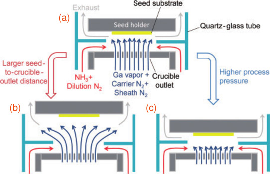
Figure 1: Schematic drawings of gas-stream pathways for Ga vapor from crucible outlet to seed substrate in cases of (a) low pressure and small seed-to-crucible-outlet distance, (b) larger seed-to-crucible-outlet distance, and (c) higher pressure (lower gas-stream velocity). Arrow length corresponds to gas-stream velocity for Ga vapor emitted from the crucible outlet.
The important growth parameters were found to be reducing the seed-to-crucible-outlet distance and decreasing the process pressure (Figure 1). The ammonia supersaturation level, as given by the ‘gas-flow-rate ratio’, had a lesser effect, mainly in affecting the amount of GaN polycrystals forming on or near the crucible outlet rather than contributing to growth on the substrate (Figure 2).
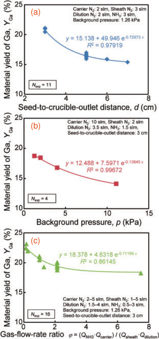
Figure 2: Dependences of material yield of Ga in HF-VPE GaN growth on (a) seed-to-crucible-outlet distance, (b) background pressure, and (c) gas-flow-rate ratio. Regression formulae were based on the exponential decay function with a y offset.
With the 2-inch substrates, the Toyota team found halogen-free VPE material yields for Ga to GaN in the range 14-23%, compared with 5-10% for hydride VPE.
Further experiments for ultra-high material yield growth were carried out on 3-inch and 4-inch diameter sapphire wafers. Here, it was hoped that more gallium would be deposited on the substrate rather than being wasted in the exhaust gases. This compensated somewhat for the limits on reducing the seed-to-crucible-outlet distance as a means to increased material yield. For the 4-inch seed substrate, the material yield increased to ~47%.
The Toyota team comments: “With this ultra-high material yield, we believe that HF-VPE can be used to produce a sufficient number of GaN wafers for high-power vertical GaN devices at moderate prices without depleting the global Ga supply.”
The result on the 3-inch seed wafer was intermediate between the 2-inch and 4-inch substrates, suggesting a linear relation.
The researchers also estimated what the material yield for halogen-free VPE would be with pressures (~100kPa) and seed-to-crucible-outlet distance (~10cm) typical of hydride VPE – the result was 7%-8%. Hence, the higher material yields come from the lower process pressure achievable with a chlorine-free chemistry. Also, the RF heating allows the gallium crucible to be heated to higher temperatures (~1200°C) than the rest of the reactor. This enabled a steep temperature gradient in the growth zone, allowing shorter seed-to-crucible-outlet distances.
https://doi.org/10.7567/APEX.11.065502
The author Mike Cooke is a freelance technology journalist who has worked in the semiconductor and advanced technology sectors since 1997.


