


- News
7 June 2018
Aluminium indium nitride as interlayer for green-emitting multi-quantum wells
Lehigh University in the USA has been using aluminium indium nitride (AlInN) as an interlayer (IL) to boost the photoluminescence (PL) intensity of indium gallium nitride (InGaN) multiple quantum wells (MQWs) in the green region of the visible spectrum [Wei Sun et al, Appl. Phys. Lett., vol112, p201106, 2018]. The MQWs with AlInN IL achieved up to 7x the PL intensity compared with MQWs without IL before the separating 10nm GaN barriers.
Green light is the most difficult to produce from semiconductor devices, compared with the red and blue components for RGB white light. Many groups have been struggling to improve heterostructures for this ‘green gap’ with a view to more efficient white emitters, compared with blue or ultraviolet light-emitting diodes used as an excitation source on phosphors. Also, direct RGB sourcing would allow versatile color temperature tuning.
The higher indium contents needed for green light-emitting InGaN give rise to problems such as phase separation, defects from large lattice mismatch strain, lower material quality from the low growth temperatures needed for higher indium incorporation, and built-in electric fields from varying charge polarization of the III-nitride bonds.
AlInN with high Al-content provides capping and smoothing effects for abrupt InGaN interfaces. Further, the material enables strain engineering, tuning from tensile to compressive stress by changing the In-content. The wider bandgap of AlInN should also suppress electron leakage, giving better carrier confinement in the wells. AlGaN has previously been used in research as an IL. While AlGaN creates tension with respect to GaN, AlIN allows strains from compression through lattice matching to tension.

Figure 1: (a) Schematic illustration of the InGaN-based multiple quantum well (MQW) structure with an AlInN barrier layer or interlayer. (b) Profile of growth temperature (Tg) and pressure (Pg) as a function of time for one period of MQW growth. Growth times not to scale.
The structures were grown using metal-organic chemical vapor deposition (MOCVD) on c-plane sapphire. The metal-organic precursors were triethylgallium (TEGa), trimethylindium (TMIn) and trimethylaluminium (TMAl), while ammonia provided the nitrogen. The GaN template consisted of an 800nm buffer grown at 1050°C and 3μm undoped material. Five-period MQW structures were grown on the template with InAlN or AlGaN interlayers (FIgure 1, Table 1). During the MQW growth sequence, the pressure and temperature were varied to optimize quality. In particular, InAlN growth required a factor of 10 lower pressure than for the other layers. The changes were carefully ramped to avoid turbulence in the chamber.
Table 1: Sample MQW structures. Barriers for all structures 10nm GaN.
| Sample | Well | Interlayer |
| A1 | 3.3nm In0.19Ga0.81N | 1nm Al0.89In0.11N |
| A2 | 3.3nm In0.15Ga0.85N | 1nm Al0.83In0.17N |
| A3 | 3.0nm In0.19Ga0.81N | 1nm Al0.89In0.11N |
| B1 | 3.3nm In0.20Ga0.80N | 0.4nm Al0.42G0.58N |
| B2 | 3.3nm In0.21Ga0.79N | 1.0nm Al0.42Ga0.58N |
| B3 | 3.3nm In0.21Ga0.79N | 1.7nm Al0.42Ga0.58N |
| C1 | 3.3nm In0.19Ga0.81N | None |
X-ray diffraction (XRD) analysis suggested that the AlInN interlayer enabled improved structures with more abrupt heterointerfaces. The researchers attribute the improvement first to the interlayer capping the wells and preventing out-diffusion of indium. Second, the tensile strain of the interlayer compensates the compressive strain of the wells, allowing pseudo-morphic growth over the five periods of the MQW structure.
The sample A1 with AlInN interlayers (ILs) had 5x more intense photoluminescence (PL), compared with the reference sample C1 without interlayers with excitation from a 400μm-diameter 405nm laser spot with 24W/cm2 power density. The spectrum of the A1 sample was broader with 44nm full-width at half maximum than the spectrum from C1 (35nm). The researchers comment: “The broadening of the PL spectrum in MQW with AlInN ILs could be attributed to the inhomogeneous growth of the MQW caused by the pressure changes and unstable growth.” The peak wavelength of both structures was 530nm.
The intensity varied with pump power. The A1 sample was 4-7x more intense over the range up to almost 1.2kW/cm2 power density, compared with C1. The intensity peaked at a lower power for A1. The team suggests that this shows “a decrease in defect or Shockley-Read-Hall recombination”.
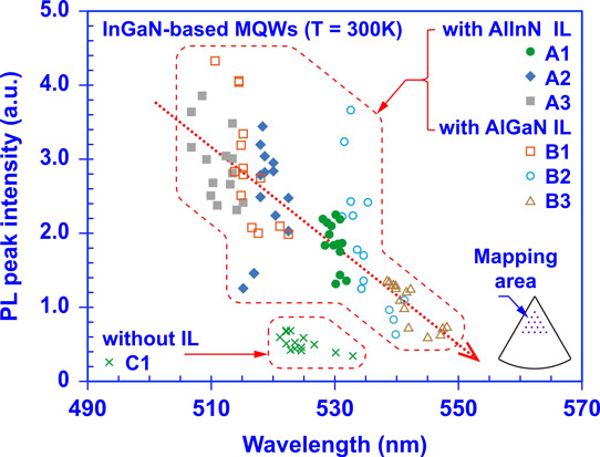
Figure 2: PL peak intensity comparison at room temperature (300K) of seven different InGaN-based MQW samples. For each MQW sample, PL spectra are mapped at 15 different spots with peak intensities plotted as function of peak wavelength.
Varying the samples more widely (Figure 2), narrower wells gave shorter wavelength, tending into the blue-green region, and higher intensity. Also, reducing the indium composition also gave shorter wavelengths and higher intensity. The AlInN interlayers gave similar performance to the more researched AlGaN structures.
AlInN InGaN MQWs Green light emission MOCVD
https://doi.org/10.1063/1.5028257
The author Mike Cooke is a freelance technology journalist who has worked in the semiconductor and advanced technology sectors since 1997.


