


- News
27 June 2018
Monolithic indium phosphide on silicon growth for optoelectronics
Hong Kong University of Science and Technology (HKUST) has been advancing technologies for direct growth of indium phosphide (InP) on silicon (Si) substrate with a view to monolithic integration of optoelectronics on a low-cost platform.
In particular, professor Kei May Lau’s group at HKUST claims the first indium gallium arsenide/indium aluminium gallium arsenide (InGaAs/InAlGaAs multi-quantum-well (MQW) lasers directly grown on on-axis V-grooved (001) Si by metal-organic chemical vapor deposition (MOCVD) [Si Zhu et al, Optics Express, vol26, p14514, 2018]. Miscut silicon substrates are often used to grow III-V materials to avoid defects such as anti-phase boundaries.
Integration of lasers with on-axis silicon is desired for the interconnection of photonic integrated circuits and optical-fiber large-scale networking with the efficient, complex complementary metal-oxide-semiconductor (CMOS) electronics that powers today’s communications technologies. Monolithic integration, it is hoped, will reduce the costs arising from additional processing needed for wafer bonding, and also allow the use of larger-diameter substrates for economies of scale.
The V-groove Si was created by etching with potassium hydroxide solution through a silicon dioxide (SiO2) mask. The parallel stripes were made with a 130nm pitch. The silicon surface was prepared for MOCVD with 800°C thermal desorption of native oxide.
The III-V growth for the laser diode (Figure 1) began with a 10nm GaAs wetting layer on the (111) facets of the grooves at 400°C. The wetting layer was found to avoid non-uniformities and large InP clusters that can be detrimental to further growth and coalescence into thin films.
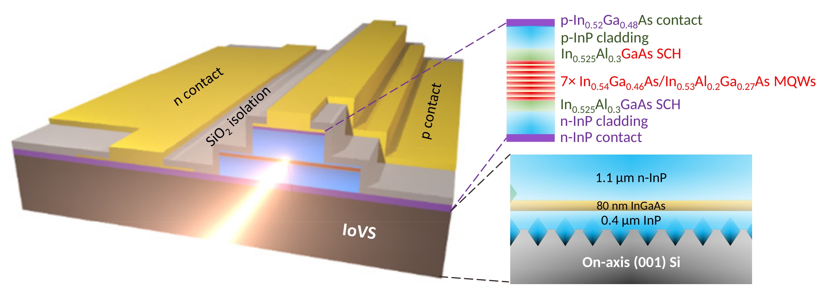
Figure 1: Schematic architecture of InGaAs/InAlGaAs MQW laser diode directly grown on on-axis (001) Si.
InP growth began with 435°C nucleation and a 540°C buffer, forming an array of nanowires. The silicon dioxide masking was removed and further 600-630°C InP growth coalesced the film into a 1.5μm-thick layer. This film included an 80nm strained InGaAs dislocation filter. The surface had a 3.31nm root-mean-square roughness, according to atomic force microscopy. There was some evidence of stacking faults with a density of 1.2x10⁸/cm2. The threading dislocation density (2.4x10⁸/cm2) was estimated to be a factor of 3.7 lower than for InP grown on planar silicon (1.1x10⁹/cm2).
The InP template was then the basis for the laser structure, with 77nm In0.525Al0.3Ga0.175As separate confinement heterostructure (SCH) waveguide layers sandwiching the InGaAs/InAlGaAs MQW active region (7x(8nm/23nm In0.54Ga0.46As/In0.53Al0.2Ga0.27As)). Cladding layers consisted of InP: 1μm upper p-type, 630nm lower n-type. The p-contact layer was 65 nm In0.52Ga0.48As. The n-InP contact layer was 120nm thick.
The material was fabricated into ridge-waveguide laser diodes. The ridge widths varied between 2μm and 70μm. The ridge consisted of a narrower mesa and a wider one around the MQW. The aim of the wider regions was to keep the current flow away for the sidewalls, avoiding non-radiative surface recombination. Electrical isolation was achieved with 500nm-thick SiO2. The p- and n-contacts were titanium/platinum/gold and germanium/gold/nickel/gold, respectively.
The final stage of the fabrication involved thinning the wafer to 100μm thick and cleaving into laser bars without surface coatings on the end facets.
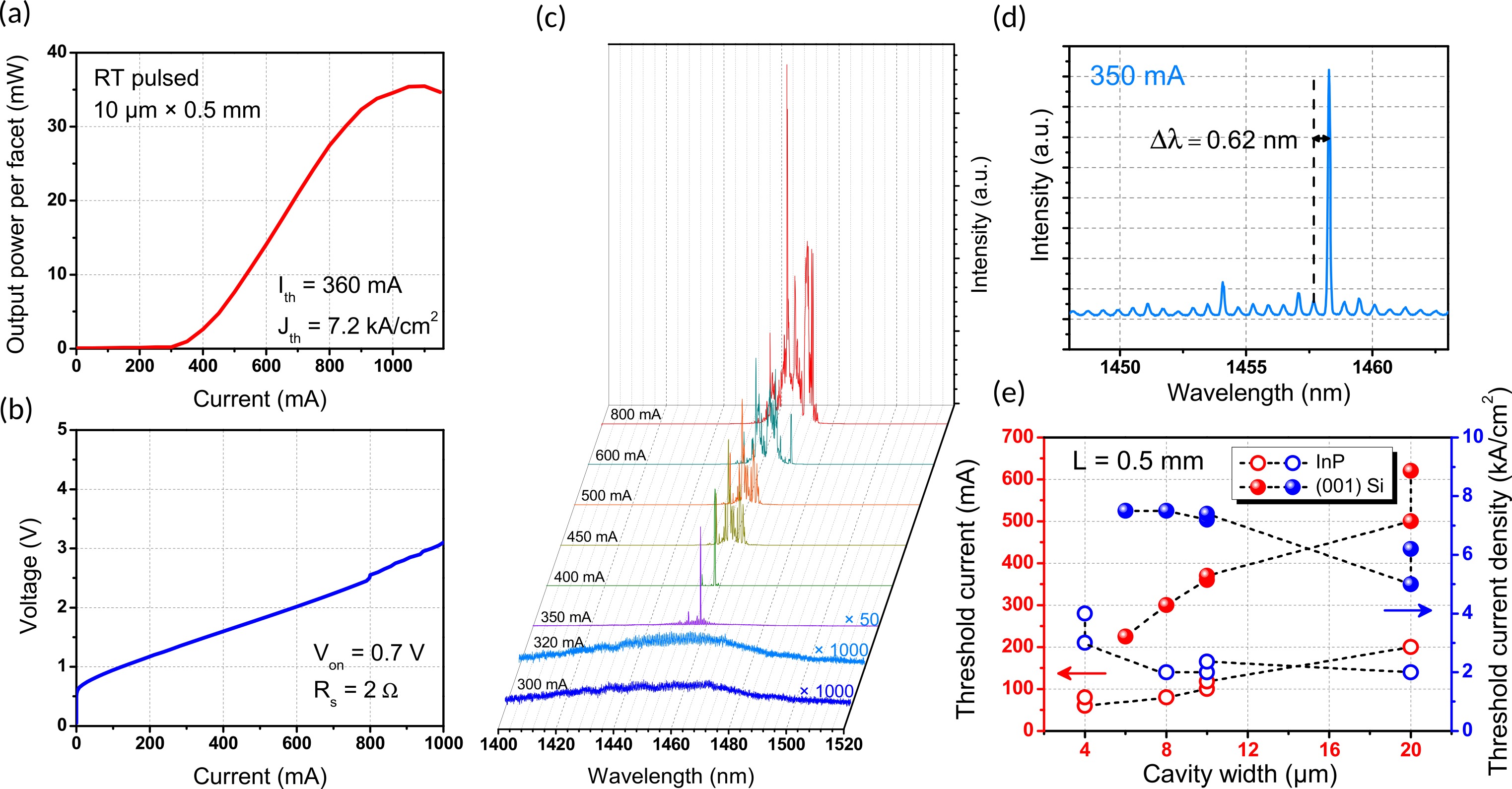
Figure 2: (a) Light output power and (b) current versus voltage characteristics for 20°C. (c) Emission spectra at various injection currents. (d) Enlarged emission spectrum at 350mA current injection. (e) Threshold current and threshold current density as function of laser cavity width with fixed cavity length of 0.5mm on (001) Si and InP substrates.
The threshold current for lasing in pulsed mode from a 10μmx0.5mm device was 360mA, which corresponds to 7.2kA/cm2 density (Figure 2). At 1A injection, the output power was 35mW per facet (70mW total).
The main emission peak was at 1.46μm wavelength, but there was some emission from higher longitudinal modes. Similar lasers produced on native InP substrates emit 1.48μm radiation. The researchers attribute the blue-shift on silicon to strain effects arising from thermal expansion mismatches between InP and Si.
Also, the threshold currents of devices on silicon were about three times higher than those produced on InP substrate. “This disparity is mainly due to the penetration of some defects through the QWs on Si, though most of them have been annihilated inside the buffer layers,” the team comments. Internal quantum efficiency assessments put the Si-based laser diodes at a 1/2.6 disadvantage compared with devices on InP. Again, defects are blamed. The researchers suggest that more dislocation-reduction approaches, such as thermal cycled growth and multiple dislocation filters (see below), could improve intrinsic performance.
Longer laser diodes allowed lower threshold current density – 3.3kA/cm2 for a 20μmx2mm device.
Performance measurements at different temperatures gave a characteristic temperature for the threshold (T0) of 133K in the range 20-40°C and 46.3K for 40-60°C. InP-based devices manage 174K for 20-60°C, 51.5K for 60-75°C and 15.1K for 75-85°C.
Kei May Lau’s group at HKUST has also reported on using quantum dots (QDs) as a potential dislocation filter in InP layers on planar silicon (IoPS) [Bei Shi et al, J. Appl. Phys., vol123, p193104, 2018].
MOCVD began with 10nm 400°C GaAs nucleation, 550°C GaAs to smooth the growth front, and 600-630°C high-quality GaAs. The growth rate increased as the temperature was raised. Next, the InP buffer was grown on the GaAs, starting at 435°C, moving through 550°C and ending with 600-630°C MOCVD.
InAs/InP QD dislocation filter layer structures (DFLs) were compared with an In0.58Ga0.42As interlayer (Figure 3). The InAs QD layers and the first part of the InP cap were grown at 510°C. The density of dots was around 3x10¹⁰/cm2. Increased numbers of QD layers were expected to “facilitate the interaction of dislocations and the strain field of the QDs, enhancing the bending effect of propagated dislocations.”
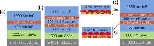
Figure 3: Schematic illustration of InP grown on planar silicon with (a) single strained InGaAs interlayer and two periods of 5-layer InAs/InP QD DFLs with dot height of (b) 2nm and (c) 5nm, respectively.
However, too many layers could lead to excessive strain that would generate new dislocations. Although theoretical considerations suggested a critical number of InAs/InP QD layers at more than 20, the researchers decided to use just two filter layers with five stacks each. The growth temperature was increased to 600°C to complete the InP cap. The samples B and C differed in the height of the low-temperature InP cap – 2nm and 5nm, respectively.
X-ray analysis suggested upper bounds to the defect density of 1.74x10⁹/cm2, 1.43x10⁹/cm2 and 8x10⁸/cm2 for samples A, B and C, respectively. Plan-view transmission electron microscopy gave corresponding threading dislocation densities of 1.2x10⁹/cm2, 5.5x10⁸/cm2 and 3.0x10⁸/cm2. Sample B suffered particularly from stacking faults, which were seen as dashes in the microscopy images. Sample C, however, suffered from regions of extended InAs islands forming during the QD growth process.
Room-temperature (RT) photoluminescence (PL) experiments were carried out on samples with an extra layer of InA/InAlGaAs QDs in 200nm InAlGaAs cladding on a 100nm InP buffer layer. Samples A, B and C were used as InP/Si templates. The structure was capped with 1.5nm InGaAs wetting layer and an uncapped layer of InAs QDs. The buried InAs QD layer was grown at 510°C and capped with 1.3nm InAlGaAs. The cladding was grown at 630°C. The dot density was 3.4x10¹⁰/cm2 on sample A and 3x10¹⁰/cm2 on C. The researchers hope that similar structures could lead to InAs QD laser diodes on silicon.
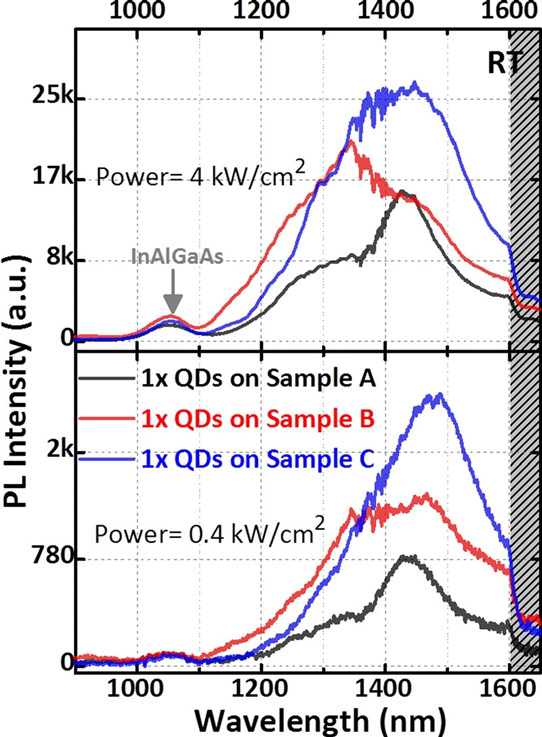
Figure 4: RT-μPL spectra of a single sheet of InAs/InAlGaAs QDs on top of the three samples in two different excitation regimes (spectra cutoff beyond 1600nm).
The QD layer on template C delivered the highest photoluminescence of all the samples (Figure 4). The linewidth for sample C was a broad 136meV, due to QD inhomogeneity with a bimodal character, giving two peaks. The higher photon energy peak increased in relative intensity at higher excitation power.
The researchers explain: “At RT, the larger QDs dominate the luminescence for two reasons: First, the carrier capture efficiency for larger QDs is higher, compared to the smaller QDs. Second, the thermally assisted tunneling of carriers via coupled excited states (CESs) contributes to the charge carrier transfer to the larger QDs from the smaller ones. However, in a high excitation regime, the excessive carriers can still easily diffuse into the smaller QDs to enhance the shorter wavelength PL emission.”
The researchers also assessed internal quantum efficiency by comparing the RT-PL with that at 20K. The RT IQEs for samples A-C were estimated at 12.2%, 13.7% and 17.3%, respectively. The researchers see progress to even better results coming from “optimizing the QD growth condition, minimizing the defect density, and improving the surface smoothness of the IoPS templates.”
InP on silicon substrate MOCVD Laser diode InGaAs InAlGaAs
https://doi.org/10.1364/OE.26.014514
https://doi.org/10.1063/1.5029255
The author Mike Cooke is a freelance technology journalist who has worked in the semiconductor and advanced technology sectors since 1997.


