


- News
29 June 2018
Schottky diodes integrated in vertical gallium nitride transistors on silicon
École Polytechnique Fédérale de Lausanne (EPFL) in Switzerland claims the first monolithic integration of vertical gallium nitride (GaN) metal-oxide-semiconductor field-effect transistors (MOSFETs) with freewheeling Schottky barrier diodes (SBD) grown on 6-inch silicon substrates by metal-organic chemical vapor deposition [Chao Liu et al, IEEE Electron Device Letters, published online 1 June 2018]. This builds on previous work [www.semiconductor-today.com/news_items/2018/jan/epfl_160118.shtml].
The researchers hope to find a lower-cost route to vertical GaN power devices than the very expensive processes based on high-price bulk or free-standing GaN substrates that are presently used in research. GaN substrates are used to avoid defects that reduce the critical electric field for breakdown. Vertical power devices should be able to handle higher voltages and currents than lateral architectures. The use of large-diameter silicon substrates should reduce costs, but growth of GaN on silicon tends to introduce many performance-killing defects.
Freewheeling diodes are used in power conversion applications to allow the flow of reverse-bias current in the off state, releasing energy stored in inductive elements. While the in-built body p-i-n diode of the EPFL structure does allow some current flow, the turn-on voltage is high, increasing losses during switching. SBDs have a much lower turn-on voltage, along with faster switching and lower resistance.
Using external discrete SBDs would increase parasitic inductance with the consequent risks of ringing and other system instabilities. Monolithic integration should reduce parasitic inductance and offer reduced footprints and simpler packaging.
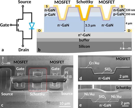
Figure 1: (a) Equivalent circuit. (b) Schematic of integrated vertical MOSFET-Schottky barrier diode (SBD). Scanning electron microscope images of (c) integrated vertical MOSFET-SBD, and (d) cross-sections of integrated vertical MOSFET, and (e) integrated vertical SBD.
The EPFL device was fabricated from an npn GaN structure on 6-inch (111)-oriented silicon (Figure 1). Plasma etching down to the n--GaN drift layer was used for 1.3μm trench structures. The surfaces of the trenches were smoothed to 0.42nm root-mean-square roughness with tetra-methyl ammonium hydroxide (TMAH) solution treatment at 85°C for 90 minutes. The SBD metal contact consisted of nickel/gold (Ni/Au). The MOSFET gate stacks used silicon dioxide (SiO2) insulation with chromium/gold (Cr/Au) metal.
The MOSFET-SBD structure was compared with reference discrete GaN MOSFETs: the saturation current densities were ~0.35kA/cm2 for both, with respective specific on-resistances of 10.1mΩ-cm2 and 12.6mΩ-cm2 (Figure 2). The resistance difference was within the on-wafer variation for devices of the same kind.
With 10V drain bias, the threshold voltages were ~+3.9V for both devices, giving enhancement-mode, normally-on behavior. Under the same conditions, the on/off current ratio was more than 108, and the subthreshold swing was ~218mV/decade. The MOSFET-SBD structure did have a slightly higher off-state leakage, but still less than 10-8kA/cm2. An increase in gate leakage from 6x10⁻¹⁰kA/cm2 to 2x10⁻⁷kA/cm2 as the gate potential was increased from 0V to 12V could be eliminated by a higher-quality, more conformal gate dielectric, according to the researchers.
With a reverse bias on the drain, the turn-on voltage is -3.7V for the body p-i-n diode. By contrast, the SBD allows current to flow even with the gate potential below threshold, and going above threshold only slightly increases the current flow.
The SBD on-voltage for a 20A/cm2 current density was 0.76V, described as “among the lowest values reported in vertical GaN diodes so far”. The specific on-resistance (RON,SP) at 8.7V forward bias was 1.6mΩ-cm2. The ideality factor at 0.4V was about 1.5. The reverse current was in the picoamp range. The team comments: “A combination of such low RON,SP and good ideality factor is a result of the excellent drift-layer quality with low defect density, high electron mobility, as well as excellent Schottky contact formed on the smooth n--GaN surface subject to TMAH treatment.”
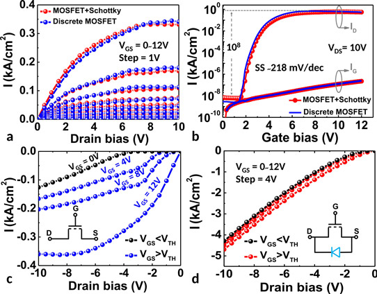
The breakdown voltages of the discrete and SBD-MOSFETs were 542V and 254V, respectively. Although the SDB-MOSFET had reduced breakdown, the team points out that the SBD had “state-of-the-art performance compared to vertical GaN-on-Si SBDs”.
Apart from using low-defect-density GaN substrates, improved breakdown performance could come from increasing the drift layer thickness and reducing background carrier concentrations, along with deploying field-plate, edge-termination and guard-ring technologies. Benefit could also be extracted from alternative architectures such as trench or junction SBDs.
GaN MOSFETs Schottky barrier diodes
https://doi.org/10.1109/LED.2018.2841959
The author Mike Cooke is a freelance technology journalist who has worked in the semiconductor and advanced technology sectors since 1997.


