


- News
18 July 2018
Improving aluminium gallium nitride transistor channel performance
Xidian University in China claims record results for aluminium gallium nitride (AlGaN)-channel high-electron-mobility transistors (HEMTs) [Ming Xiao et al, IEEE Electron Device Letters, published online 18 June 2018]. The improved performance covers high maximum drain current, low gate leakage current, low off-state drain current, high on/off current ratio (Ion/Ioff), high maximum transconductance, and high electron mobility. The researchers say that these are the best results to date of any other AlGaN-channel HEMT reported in the literature.
The team comments: “These results not only drastically reduce the performance gaps between the AlGaN-channel HEMT and the GaN-channel HEMT in the maximum drain current, the maximum transconductance and the electronic mobility, but also demonstrate better performances in the gate leakage current, the off-state drain current, Ion/Ioff ratio, and the breakdown voltage.”
In principle, the wider bandgap of AlGaN compared with conventional GaN-channel HEMTs should give higher breakdown voltages, indicating potential for power conversion applications. However, development is at an early stage and AlGaN channels presently have lower electron mobility and sheet density than GaN, impacting performance.

Figure 1: Device structures: (a) AlGaN-channel HEMT and (b) GaN-channel HEMT.
The researchers fabricated HEMT devices using materials with AlGaN and pure GaN channels (Figure 1). For the AlGaN channel, metal-organic chemical vapor deposition (MOCVD) on sapphire produced a three-stage AlGaN buffer, starting with 1μm of GaN, then 500nm of graded AlGaN, and finishing with 200nm of Al0.10Ga0.90N. The barrier layers consisted of a 2nm AlN spacer, 12.5nm of Al0.35Ga0.65N, and a 2nm GaN cap. The GaN comparison device had an Al0.25Ga0.75N barrier layer.
The graded AlGaN part of the buffer was designed to adjust stress and improve crystal quality. The two-dimensional electron gas (2DEG) channel that formed near the buffer/barrier junction has a Hall sheet electron density of 6.1x10¹²/cm2 and mobility of 807cm2/V-s. The mobility value is lower than that typically achieved in GaN channel material, but higher than previously reported for AlGaN channels. Alloy disorder in AlGaN tends to reduce mobility.
HEMT fabrication included dry-etch mesa isolation, annealed ohmic source/drain contacts of titanium/aluminium/nickel/gold, and 60nm of plasma-enhanced chemical vapor deposition (PECVD) silicon nitride passivation. The 1μm-long gate was nickel/gold, placed 1.5μm from the source contact.
With the gate at -10V, giving an off state, the drain current with 16V bias was 0.96nA/mm for the AlGaN channel, comparing with 69nA/mm for the conventional GaN HEMT. The gate leakages were 1.37nA/mm and 112nA/mm, respectively. The Ion/Ioff was 0.93x10⁹ for the AlGaN channel, and 1.3x10⁷ for a GaN channel.
The researchers explain: “For AlGaN-channel devices, low off-state drain current and high Ion/Ioff resulted from the low gate leakage current because the AlGaN channel material has deeper energy-level traps and lower background carrier concentration than the GaN channel material.”
For positive gate potential, the gate leakage continued to be lower for the AlGaN HEMT – the gate potential was ~2.1V higher than for a GaN channel with a 40mA/mm gate current. Thus, AlGaN channels should allow a wider operating range in terms of gate voltage. The maximum drain current was 849mA/mm with 500ns pulses and 10ms cycle for the quiescent point of -4V gate potential and +8V drain voltage. Pulsed operation was used to avoid thermal performance degradation since the sapphire substrate has low heat conductivity. In the same tests the peak transconductance was 108mS/mm.
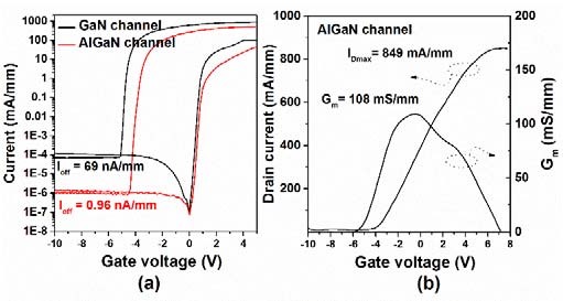
Figure 2: (a) Semilog DC transfer characteristic and gate leakage current curves and (b) linear gate-pulse transfer characteristic and transconductance curves of 1.5μm gate-drain HEMTs at 16V drain bias.
The team comments that the maximum drain current is the largest in reported AlGaN-channel HEMTs due to the high electronic mobility of 807cm2/V-s and the high saturated electronic velocity. The improved material performance is attributed to high AlGaN/AlGaN heterostructure quality.
The gate-drain distances of the devices were varied between 1.5μm and 20μm. Longer distances mean higher on-resistance, but in compensation allow higher drain biasing without breakdown. The on-resistance varied between 6.1Ω-mm and 28.8Ω-mm, respectively, for the 1.5μm and 20μm gate-drain distances. With the gate at +6V, the saturation drain current exceeded 800mA/mm for all the devices.
Off-state (gate at -10V) breakdown voltages for 1.5μm and 5μm gate-drain distances were 150V and 408V, respectively. For GaN-channel HEMTs the corresponding values were 110V and 302V. The researchers point out that the devices did not have any breakdown-increasing features such as field plates or Schottky-source/drain contacts.
https://doi.org/10.1109/LED.2018.2848661
The author Mike Cooke is a freelance technology journalist who has worked in the semiconductor and advanced technology sectors since 1997.


