


- News
23 July 2018
KAUST demonstrates nanowire GRINSCH diode for efficient UV-LED/laser applications
© Semiconductor Today Magazine / Juno PublishiPicture: Disco’s DAL7440 KABRA laser saw.
AlGaN-based light-emitting devices are promising ultraviolet light sources to replace the existing UV gas lasers and UV lamps containing toxic substances (mercury). However, the performance of AlGaN-based UV emitters are limited, and in particular high-power UV laser diodes (emitting below 330nm) have not yet been reported. Moreover, the threshold operating voltages of reported UV laser diodes (>330nm) are quite high, surpassing 25V in lasing mode with high series resistance due to poor hole injection efficiency.
These limitations in device performance are attributed to several factors such as the presence of a high density of defects (dislocations) and inefficient p-type doping of the Al-rich AlGaN layers, and the lack of efficient thermal dissipation channels for existing device schemes. A new device scheme is therefore urgently needed.
AlGaN nanowires, however, are found to be promising candidates to overcome these obstacles. Compared with AlGaN epitaxial thin-film layers, defect-free AlGaN nanowires can be grown directly on many substrates (including metals) due to the efficient strain relaxation associated with the large surface-to-volume ratio. The metal or metal-coated silicon or sapphire substrates can offer better heat dissipation channels for high-current operation. Furthermore, p-type nanowires (Si, Ge, GaN, etc) have been recognized as having relatively low resistivity due to more efficient magnesium (Mg) incorporation and lower activation energy. Hence, the development of UV sources made of AlGaN nanowires has been a field of great interest.
Recently, a team at Sausi Arabia’s King Abdullah University of Science and Technology (KAUST), led by Haiding Sun, Xiaohang Li, Boon S Ooi and others, proposed for the first time a novel dislocation-free nanowire structure with a graded-index separate-confinement heterostructure (GRINSCH) configuration in which they embed an active region between two compositionally graded AlGaN layers, namely a GRINSCH diode (Sun et al ‘Graded-Index Separate Confinement Heterostructure AlGaN Nanowires: Toward Ultraviolet Laser Diodes Implementation’, ACS Photonics, DOI: 10.1021/acsphotonics.8b00538).
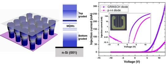
Picture: 3D schematic of fabricated nanowire GRINSCH UV emitters and I-V curves of the GRINSCH and conventional p-i-n diodes.
Extensive theoretical and experimental work has demonstrated that such diodes possess superior electrical and optical performance. The calculated electronic band diagram and carrier concentrations show the automatic formation of a p-n junction with electron and hole concentrations of ~1018/cm3 in the graded AlGaN layers even without intentional doping. A significantly lower turn-on voltage of 6.5V (reduced by 2.5V) and smaller series resistance of 16.7Ω (reduced nearly four-fold) are achieved in the GRINSCH diode (see Figure) compared with the conventional p-i-n diode.
Such an improvement in electrical performance is attributed mainly to the introduction of compositionally graded AlGaN layers enhancing the transport properties of the electron and holes due to the polarization-induced n- and p-doping. Furthermore, a better carrier distribution (both electrons and holes) with large optical confinement have also been verified. They therefore believe that the GRINSCH diode could offer an unconventional path for developing solid-state UV optoelectronic devices, mainly future laser diodes.
Ultimately, low defect/dislocation density, low turn-on voltage and small sheet resistance, and better heat dissipation channels are the key prerequisites for achieving high-performance III-nitride based UV and visible devices. The proposed device scheme possesses:
(1) no dislocation of the structure;
(2) less efficiency droop by adopting Ti/TaN metal-bilayer coated-Si substrates,
(3) significantly improved I-V characteristics by taking advantage of the polarization-induced doping; and
(4) better carrier and optical confinement (crucial for laser structure).
Previously, such a GRINSCH diode configuration has been successfully implemented in conventional III-V-based (e.g. GaAs, InP) laser diodes, by virtue of the simultaneous improvement of carrier injection and vertical optical mode confinement. A UV laser diode design with a GRINSCH configuration can therefore take advantage of the polarization-enhanced p-type doping while achieving better carrier and optical mode confinement.
The researchers anticipate that this structure, particularly the demonstration of the effectiveness of polarization-induced n- and p-doping, will find broad practical application in fabricating self-assembled nanowire-based high-efficiency devices, such as lasers, photodetectors, modulators and photonic integrated circuit (PIC)-related devices.


