


- News
29 January 2018
Questioning carrier distributions in III-nitride light-emitting diodes
University of Bath and University of Cambridge in the UK have reinterpreted the ABC model of recombination in indium gallium nitride (InGaN) multiple quantum well (MQW) light-emitting diodes (LEDs) to suggest that the carrier distribution across the wells is more uniform than presently believed [M. A. Hopkins et al, J. Appl. Phys., vol122, p234505, 2017]. In particular, the reinterpreted model is used to study the variation of the modified constants with the number of wells of fabricated LEDs.
Non-uniformity of the hole carrier distribution is thought to be one cause of efficiency droop in InGaN LEDs at high current. Drift-diffusion transport of carriers is used to explain the non-uniformity. The researchers comment on their results against the consensus: “The implications of the reported results are that drift-diffusion plays a far lesser role in cross-well carrier transport than previously thought; that the dominant cause of efficiency droop is intrinsic to the quantum wells and that reductions in the density of non-radiative recombination centers in the MQW would enable the use of more QWs and thereby reduce Auger losses by spreading carriers more evenly across a wider emissive region.”
The ABC model uses three parameters, A-B-C, to describe the radiative recombination of injected carriers. The desired radiative recombination of electrons and holes into photons is related to the B-term, which is proportional to the product of the electron and hole densities. The A-term, proportional to the minority carrier density, is related to Shockley-Read-Hall recombination through intermediate defect energy levels in the bandgap. The final C-term, where one of the densities is given a single power and the other is squared, is traditionally attributed Auger processes where electron-hole recombination is aided by energy transfer to another carrier. However, there are also other explanations given for the C-term.
The researchers grew blue 2.4nm/7.0nm InGaN/GaN MQWs by metal-organic chemical vapor deposition (MOCVD) on c-plane sapphire. The material had a threading dislocation density of around 4x10⁸/cm2. The barriers were grown in two temperature steps, first ramping to 846°C after the In0.12Ga0.88N well deposition, and then increasing to 880°C for most of the growth.
The layers before the MQW active region consisted of 2.0μm GaN, 2.5μm n-GaN, 23nm In0.05Ga0.95N, and 3nm GaN. After the MQW came a 12nm p-Al0.17Ga0.83N electron-blocking layer and a 120nm p-GaN layer.
Lateral 420μmx400μm devices were fabricated with annealed nickel/gold interdigitated electrodes for more uniform current spreading across the LED. To further equalize the current density across the device, a thin nickel layer was deposited on some of the electrode and p-contact structures. The effect of the extra nickel layer was small and had little effect on the subsequent ABC modeling. The researchers comment: “From this, we conclude that non-uniform current spreading had little influence on the efficiency droop observed in our LEDs.”
The mesa and transparent p-GaN contact areas were 1.48x10⁻³cm2 and 1.17x10⁻³cm2, respectively. The number of wells varied between 3 and 15. The researchers found that devices with more wells suffered from less droop in external quantum efficiency (EQE) at high current.
The researchers applied the ABC model to their results with provision for tunneling and overflow currents. Unlike most modeling, the team considered that the photon-emitting recombining carriers were spread across the wells rather than restricted to the wells near the p-contact end. Hence they expected their αβγ modified coefficients would have different proportionalities to the number of wells (N, Figure 1).
The team suggests that, under forward bias, electrons and holes are injected into the superlattice-like band-like states arising from the periodic structure of the QWs. “Such direct carrier injection into the superlattice-like states of the quasi-sawtooth band profile is likely to promote still further rapid transport of both electrons and holes to yield more nearly uniform steady-state distributions across the MQW,” they write. The saw-tooth potential profile arises from the charge polarization changes of the different c-plane III-nitride layers, giving rise to electric fields.
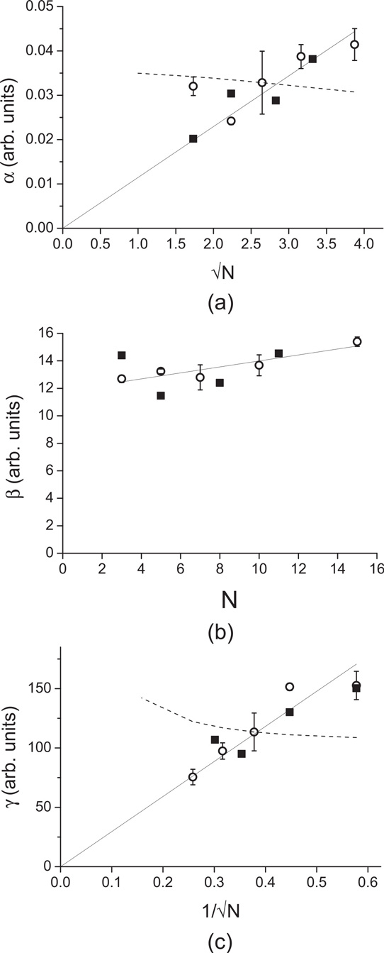
Figure 1: (a) α versus √N, (b) β versus N, and (c) γ versus 1/√N. Open-circle data points obtained from fits to EQE measurements. Black lines are straight line fits to results. Trend lines forced through origin for α (3-well point excluded) and γ. Closed-square symbols are from fitting of data of Zhang et al (excluded from trend line fitting). Dashed lines in (a) and (c) show trends that would be seen if exponentially decaying distributions of electrons and holes occur in MQW.
The researchers sought further confirmation of their ideas by fitting the results of another group to the model [Zhang et al, Opt. Express, vol23, pA34, 2015]. Also, they developed a model to reflect the more usual drift-diffusion mechanism with non-uniform carrier distributions (dashed lines in Figure 1).
Of course, the idea that the carrier distribution is non-uniform is not just due to simulations. Some experiments have varying well widths to give different wavelength emissions to help determine carrier distributions empirically. The team comments: “The presence of a deeper or wider QW in a superlattice or MQW will both introduce electron and hole states localized to the different wells and disrupt the formation of the quasi-extended states by which free carriers would otherwise spread through the MQW by thermally assisted tunneling.”
The researchers believe that the cause of drooping is intrinsic to the MQWs, giving three possible mechanisms: “Auger recombination, carrier density activated defect recombination (DADR), and tunneling-assisted non-radiative recombination, the latter including trap-mediated Auger effects.” They add that their results do not enable them to distinguish the primary mechanism from this menu. For semi-polar/non-polar LEDs, the contribution of thermally assisted tunneling could be reduced or even absent.
https://doi.org/10.1063/1.4986434
The author Mike Cooke is a freelance technology journalist who has worked in the semiconductor and advanced technology sectors since 1997.


