


- News
15 January 2018
SMI demos MOCVD growth of silicon-doped gallium oxide on sapphire substrates
© Semiconductor Today Magazine / Juno PublishiPicture: Disco’s DAL7440 KABRA laser saw.
Structured Materials Industries Inc (SMI) of Piscataway, NJ, USA – which provides chemical vapor deposition (CVD) systems, components, materials, and process development services – says that its R&D team has grown silicon-doped gallium oxide (Ga2O3) films on sapphire (Al2O3) substrates using metal-organic chemical vapor deposition (MOCVD). The demonstration proves that doped Ga2O3 films can be deposited uniformly on large-area substrates for device applications, says the firm.
Previously, SMI grew Si-doped Ga2O3 films on insulating (or unintentionally doped) bulk Ga2O3 substrates that were acquired from different organizations around the world, including IKZ in Germany, Tamura in Japan, and Synoptics in California.
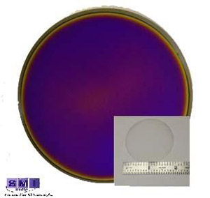 Image: An 8” silicon wafer with Ga2O3 deposited on it. Similar products will be made available in smaller wafer sizes.
“We chose gallium oxide (Ga2O3) as a wide-bandgap semiconductor material because of its impressive properties which, for certain applications, are widely regarded as superior to silicon (Si), silicon carbide (SiC) and gallium nitride (GaN) semiconductor materials,” says Dr Serdal Okur, principal investigator for SMI’s Department of Energy (DOE) and National Aeronautics and Space Administration (NASA) Ga2O3 projects. “There is a significant amount of commercial opportunity for Ga2O3 on Al2O3. One example is a low-cost power control device based on a superior wide-bandgap semiconductor material, which could add benefits of higher-voltage, higher-power-handling, and higher-frequency capabilities,” he adds. “In addition, tuning the energy bandgap of Ga2O3 with Al2O3 and In2GaO3 enables a broad range of applications such as photodetectors tunable through UV wavelengths, optical filters with tunable transmission range, and graded heterostructures for optoelectronic devices, as well as MOSFETs,” Okur notes.
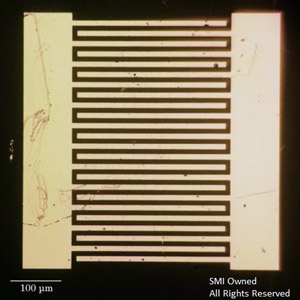 Image: Optical micrograph of interdigitated contact pattern on Ga2O3 epilayer grown on Al2O3.
“We are very proud to offer high-quality customized solutions for new material efforts that enable researchers to meet their developmental objectives,” says president & CEO Dr Gary S. Tompa. “This offering comes as an extension from our traditional line of products and the commercialization of technologies funded by the government while collaborating with notable universities and companies in the United States,” he adds. “This milestone achievement executed by our research team attests to our company's strategic objectives and core competencies.”
The materials were grown using in-house SMI-fabricated MOCVD tools. The Ga2O3 was grown in one of the firm’s two Ga2O3 MOCVD reactors, one of which features a rotating disc reactor with a 13”-diameter susceptor. The other features single 2”-wafer processing through 1200°C.
SMI can provide tools to grow Ga2O3 on Al2O3 and/or the materials in research-size quantities. Ga2O3 film on Al2O3 substrates will be available for purchase on SMI’s website in wafer sizes of 2”; joining the firm’s already available homoepitaxy doped and undoped Ga2O3 films. SMI says that the product is suitable for researchers and industry professionals aiming to develop power devices and sensors.
SMI recruits scientists to expand MOCVD, ALD and HVPE product development


