


- News
12 January 2018
US Army and Stony Brook grow InAsSb on GaAs substrates using GaSb intermediate defect-trapping layer and graded buffer
© Semiconductor Today Magazine / Juno PublishiPicture: Disco’s DAL7440 KABRA laser saw.
The US Army Research Laboratory (ARL) and Stony Brook University (funded by the Army Research Office) have developed a new synthesis process for the low-cost fabrication of a material previously discounted for high-sensitivity infrared cameras, opening new possibilities for future Army night-time operations (‘Bulk InAsSb with 0.1 eV bandgap on GaAs’, Journal of Applied Physics 122, 025705 (2017)).
ARL’s Drs Wendy Sarney and Stefan Svensson led a novel approach to using the III-V compound semiconductor material indium arsenide antimonide (InAsSb), which is used in optoelectronics in many commercial products (such as DVD players and cell phones) but has not been used before in high-performance IR cameras for the longest wavelengths (10μm). The best materials for the IR camera light-sensors are currently based on the II-VI compound semiconductor material mercury cadmium telluride (HgCdTe). “Unfortunately, they are very expensive, mostly because there are only military customers for this material,” says Svensson.
“The human eye is optimized by nature to observe reflected light from the sun in a very narrow band of colors… the visible spectrum; however, all objects in nature glow with a faint light even at low temperatures, which produces colors in the infrared range which are invisible to the naked eye. These wavelengths are about ten times longer than those of visible light,” he adds.
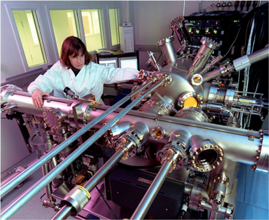
Picture: Dr Wendy Sarney using the MBE reactor at ARL to produce IR detector materials using a new synthesis process. Credit: US Army.
“By using cameras that can see the faint IR light, soldiers can operate during night times,” Sarney says. “The more sensitive such a camera is, or in other words, the smaller the color or temperature differences are that it can see, the more details that can be discerned on a battlefield and enemies can be detected at longer ranges. High-performance IR cameras are therefore extremely important for the Army.”
Key to the development was realizing that the material needed to be undistorted by strain in order to see at 10μm. This was a major difficulty that had to be overcome before InAsSb could be used as a sensor material. The performance of devices based on semiconductor materials also depends on the material’s crystalline perfection. Since InAsSb is deposited onto a substrate that has a smaller spacing between the atoms, this crystal lattice mismatch must be managed carefully for the light-sensitive material to work properly.
Among possible substrates, larger and cheaper ones typically have progressively smaller atomic spacing. Over several years ARL and Stony Brook found a way to manage the lattice mismatch, culminating in the current work which uses gallium arsenide (GaAs) as a substrate.
ARL and Stony Brook combined strain-mediating techniques to effectively manage the ~10% atomic spacing mismatch between the InAsSb sensing material and GaAs substrate. To do this, they deposited an intermediate layer of GaSb onto GaAs in a way that trapped most of the defects caused by the size mismatch. They then further increased the atomic spacing with a graded layer that also kept defects away from the InAsSb sensor material.
The material was examined with high-resolution transmission electron microscopy (HR-TEM) to make sure it had sufficient structural quality. They also found that the optical quality related to detection properties was remarkably high.
As the most common substrate used in the III-V industry for numerous consumer products, GaAs is inexpensive and available in large sizes. Large-area substrates allow manufacturing of multiple camera sensors simultaneously, which can be done in commercial foundries. This also opens up opportunities to produce high-quality IR cameras at a much reduced cost.
The research hence shows a path to a practical, lower-cost solution for the eventual fielding of night-vision systems based on III-V long-wavelength infrared materials.
http://aip.scitation.org/doi/abs/10.1063/1.4993454
www.stonybrook.edu/commcms/electrical/research


