


- News
14 February 2018
Continuous-wave operation of semi-polar blue laser diodes
University of California Santa Barbara (UCSB) in the USA has improved the continuous wave (CW) performance of semi-polar blue laser diodes (LDs) on (20-2-1) gallium nitride (GaN) by using a thin p-type layer in combination with an indium tin oxide (ITO) transparent conductor electrode as top cladding [Shlomo Mehari et al, Optics Express, vol26, p1564, 2018]. This enabled laser output powers up to 1.1W per facet, and a wall-plug efficiency of 15%.
Although III-nitride laser diodes are already applied in projection displays and optical data storage systems, wider use is hampered by high operating voltage, poor differential efficiency, and resulting low wall-plug efficiency. To avoid self-heating reduction in efficiency, pulsed operation is used. The researchers hope that development of CW operation could open up high-intensity lighting applications such as automobile headlamps and industrial illumination.
Improved differential efficiency can be attained by semi-polar laser diodes, compared with the more usual polar c-plane devices, from higher indium incorporation and better electron-hole wavefunction overlap, but operating voltages remain high. The high voltage implies high power losses, which give rise to high junction temperature and further reduction in efficiency.
The UCSB team thinned the p-type GaN and used a low-refractive-index transparent conductive oxide (TCO) as cladding in the hopes of reducing the operating voltage.
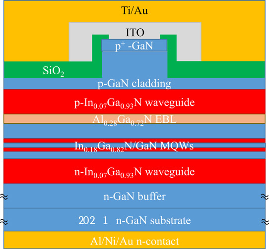
Figure 1: Schematic cross section of fabricated laser diodes with ITO p-contact layer.
The epitaxial structure for the laser diode (Figure 1) was grown on (20-2-1) free-standing GaN supplied by Mitsubishi Chemical. The active light-emitting region was a pair of 3.5nm quantum wells with 7nm barriers, grown by 840°C metal-organic chemical vapor deposition (MOCVD). After a 15nm top barrier, the p-type layers were grown at 1000°C.
Ridge-waveguide lasers were fabricated with 230nm sputtered silicon dioxide (SnO2) and 150nm electron-beam evaporated indium tin oxide (ITO) and titanium/gold p-contact structure. The facets were formed by a combination of wet etching and chemically assisted ion beam etching. There was no coating on the facets. Electron-beam evaporation was also used to deposit the back n-contact. The samples were soldered to a copper block for testing.
Reducing the p-GaN thickness from 650nm to 250nm reduced the operating voltage from 7.3V to 5.35V, respectively, for 10kA/cm2 current through the laser diode. “This low operating voltage is much lower than previously reported for blue laser diodes on semi-polar GaN substrates, and is comparable to highly optimized c-plane laser diodes,” the team comments.
The voltage efficiency for photons of 430nm wavelength was 54% for 250nm p-GaN, compared with 40% for the 650nm layer. The wall-plug efficiency was 14% for 250nm p-GaN and 10.9% for 650nm.
The researchers point out that not all the improvement comes from the reduced series resistance of the thinner 250nm p-GaN layer. They suggest that at higher biases Schottky barriers may become thinner, allowing for tunneling effects to contribute to increased current flow.
The light output power performance of the devices was very similar under pulsed operation. The threshold current density was 2.2kA/cm2. The thinner p-GaN allowed higher power under CW operation as a result of reduced heat dissipation. The peak CW light output was 0.55W for 650nm p-GaN and 0.76W for 250nm.
Infrared thermography showed a reduced average temperature in the ridge at 58°C for 250nm p-GaN for 1A current (14kA/cm2 density), compared with 85°C for 650nm. The researchers comment: “This temperature is much lower than the previously reported peak temperature of 70°C for c-plane blue laser diodes mounted on a submount and tested at drive current of 0.1A (6.2kA/cm2).”
The differential efficiency of the laser diodes with 650nm p-GaN was slightly higher than that of the 250nm laser diodes. The team believes that the difference suggests “some modal overlap with the ITO, which has a high material optical loss”. The researchers believe that improved performance could be obtained by using a lower-absorption transparent conductive material such as zinc oxide.
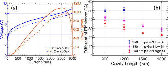
Figure 2: (a) CW light-current-voltage characteristics of 8μmx1200μm laser diodes with p-GaN thicknesses of 250nm and 150nm and lower Si doping. (b) Comparison of differential efficiencies for laser diodes with 250nm and 150nm p-GaN thicknesses and low and high Si doping levels.
Reducing the silicon doping in the n-type layers (Figure 2) allowed an increase in wall-plug efficiency to 15% at 0.96A (10kA/cm2) and peak output power of 2.2W (1.1W from each facet, current ~2.5A). The lasing wavelength in this case was 445nm.
Semi-polar blue laser diodes GaN Indium tin oxide
https://doi.org/10.1364/OE.26.001564
The author Mike Cooke is a freelance technology journalist who has worked in the semiconductor and advanced technology sectors since 1997.


