


- News
28 February 2018
Tri-anode/slant-gate gallium nitride Schottky barrier diode on silicon
Jun Ma and Elison Matioli of École polytechnique fédérale de Lausanne (EPFL) in Switzerland have used a hybrid tri-anode/slanted tri-gate structure to reduce leakage current and increase breakdown voltages in gallium nitride (GaN) lateral Schottky barrier diodes (SBDs) produced on silicon substrates [Appl. Phys. Lett., vol112, p052101, 2018].
Ma and Matioli comment: “The hybrid tri-anode pins the voltage drop at the Schottky junction (VSCH), despite a large applied reverse bias, fixing the reverse leakage current (IR) of the SBD.” They see the devices as having potential for power converters with high performance and competitive cost.
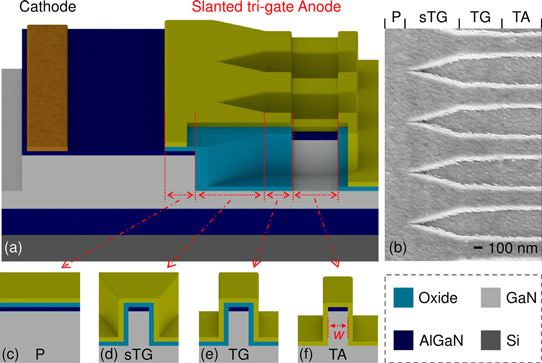
Figure 1: (a) Schematic of slanted tri-gate SBD and (b) top-view scanning electron microscopy (SEM) image of anode region. Cross-sectional schematics of (c) planar (P), (d) slanted tri-gate (sTG), (e) tri-gate (TG), and (f) tri-anode (TA) regions comprising anode.
The researchers used templates with an aluminium gallium nitride (Al0.25Ga0.75N) barrier and 5μm GaN buffer on silicon substrate. The slanted tri-gate SBD structures were etched to a depth of 180nm with inductively coupled plasma (Figure 1). The width in the anode region was 200nm. The slanted tri-gate region increased from 200nm up to 600nm towards the cathode.
The 60μm-wide devices were isolated with mesa etching. The ohmic cathode consisted of alloyed titanium/aluminium/titanium/nickel/gold. After cathode formation, 10nm of silicon dioxide and 10nm of aluminium oxide were deposited. The oxides were removed and replaced with nickel/gold to form the 4μm-long Schottky tri-anode. The nickel/gold also formed a 1.3μm-long planar single gate, 0.7μm slanted tri-gate, and 0.5μm tri-gate leading into the anode.
The researchers modeled the devices as a tri-anode SBD connected in series with a tri-gate, a slanted tri-gate, and a planar-gate transistor. The slanted and planar gate sections also operate as field plates, designed to increase breakdown voltage.
Devices with anode-cathode distances of 15μm and 25μm demonstrated, respectively, 14Ω-mm and 22Ω-mm on-resistance at room temperature. These respective values increased to 28Ω-mm and 37Ω-mm at 150°C. The 1mA/mm on-voltage was as low as 0.61V. The ideality was 1.40 at room temperature and 1.27 at 150°C.
Under reverse bias, the devices pinched-off around -1.7V. Increasing the magnitude of the reverse bias to -650V did not change the ~5.5nA/mm leakage (IR) significantly. At -830V, the leakage was still only 10nA/mm. Ma and Matioli add: “Extremely low IR of 51±5.9nA/mm was observed at -1000V, which is significantly smaller than in any other reports of GaN-on-Si SBDs.”
The leakage was increased by around 50nA/mm at 150°C. For -200V, the reverse current of 57±13nA/mm is claimed to be the smallest value among reported lateral GaN SBDs at such a high temperature.
The 1μA/mm breakdown points came at -1450V and -2000V, respectively, for the 15μm and 25μm anode-cathode devices with floating substrate bias. The corresponding hard breakdown voltages (VBR) were -1500V and -2500V. The researchers estimate the critical field at 1MV/cm. Grounding the substrate gave a unified 1μA/mm breakdown of -1060V with hard failure at -1200V.
The performance puts the shorter device in the frame for 600V/650V applications, while the longer devices could handle 1200V ratings with ~100% safety margin.
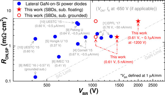
Figure 2: RON,SP versus VBR benchmark of slanted tri-gate SBDs against state-of-the-art lateral GaN-on-Si SBDs.
The researchers compared their breakdown voltage and specific on-resistance (RON,SP) results with other reports (Figure 2). The team also gives a high power figure of merit of 1.16GW/cm2 (VBR2/RON,SP).
GaN Lateral Schottky barrier diodes Silicon substrates
https://doi.org/10.1063/1.5012866
The author Mike Cooke is a freelance technology journalist who has worked in the semiconductor and advanced technology sectors since 1997.


