


- News
3 December 2018
OIP4NWE project to create open-innovation photonics pilot line
The €13.9m project OIP4NWE (Open-Innovation Photonics pilot for North West Europe) has kicked off, supported by the Interreg North-West Europe (NWE) European Territorial Cooperation Program (which is based on the cooperation of organizations from eight countries: Belgium, France, Germany, Ireland, Luxembourg, The Netherlands, Switzerland and the UK).
The project has €8.3m in funding from the European Commission via the European Regional Development Fund (ERDF) plus €5.6m from participating parties. These are led by Eindhoven University of Technology (in collaboration with its Photonic Integration Technology Center) joined by companies Aixtron SE (Germany), SMART Photonics, VTEC Lasers & Sensors, Technobis Fibre Technologies (all Netherlands), mBryonics Ltd (Ireland) and Oxford Instruments Nanotechnology Tools Ltd (UK) along with research centers Photonics Bretagne (France), Cluster NanoMikroWerkstoffePhotonik (Germany) and Photon Delta Cooperatie (Netherlands).
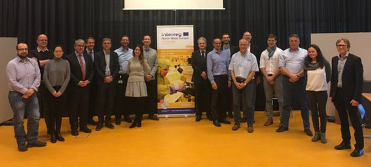
Picture: Representatives of the parties involved at the kick-off meeting in Eindhoven.
Compared with electronics, photonics uses much less energy, is faster and opens up new opportunities. A key problem that photonics can help to tackle is the exploding energy consumption of data centers, as photonic chips consume much less energy. Another example is a high-precision monitoring system for aircraft wings, bridges or tall buildings.
After two decades of basic photonics research, the first companies producing photonic integrated circuits (PICs) are taking off, but sparsely. Innovative small- and medium-sized enterprises (SMEs) are at the forefront of photonics development, but a major hurdle is the high cost of R&D. Apart from needing expensive cleanroom equipment, existing PIC production processes still have a high defect rate and are too slow. This was workable for basic research but not for commercial R&D. The technology readiness level (TRL), which ranges from 1 to 9, needs to be raised from the current 4 to 7.
The OIP4NWE project will create an efficient open-access pilot-production line for shared use by European SMEs, reducing the defect rate in pilot production and shortening throughput time. This should lead to a cost reduction that significantly lowers the threshold for developing new photonic products. The target is to help establish many integrated photonics firms and thousands of jobs within ten years of the project.
The front-end process (producing PICs on wafers) will be realized in the existing NanoLab@TU/e cleanroom at Eindhoven University. The PICs of different companies will be combined on one multi-project wafer (MPW) to keep costs low. The back-end process will be performed at the Vrije Universiteit Brussel (optics for beam shaping and light coupling) and at the Irish Tyndall National Institute (assembly of fiber-optic connections and electronics in the package). All steps require nanoscale precision to avoid product defects.
The first stage of the project is equipment installation. The second stage focusses on automation of the equipment. A third stage will involve intensive industrial research together with equipment manufacturers to optimize and develop new processes. The line should be fully in operation in 2022. To incentivize initial uptake by SMEs, a voucher scheme for external SMEs will be established.
www.tue.nl/en/research/research-areas/integrated-photonics/


